8
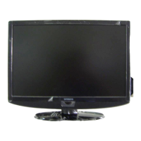
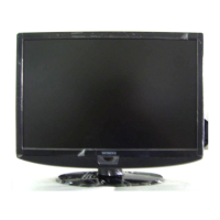
22” TFT TV Service Manual
11.6. SST37VF040
11.6.1. Description
The SST37VF512/010/020/040 devices are 64K x8 / 128Kx8 / 256K x8 / 512K x8 CMOS, Many-Time
Programmable (MTP), low cost flash, manufactured with SST’s proprietary, high performance CMOS
Super Flash technology. The split-gate cell design and thick oxide tunneling injector attain better reliability
and manufacturability compared with alternate approaches. The SST37VF512/010/020/040 can be
electrically erased and programmed at least 1000 times using an external programmer, e.g., to change the
contents of devices in inventory. The SST37VF512/010/020/040 have to be erased prior to programming.
These devices conform to JEDEC standard pinouts for byte-wide flash memories. Featuring high
performance Byte-Program, the SST37VF512/010/020/040 provide a typical Byte-Pro-gram time of 10 µs.
Designed, manufactured, and tested for a wide spectrum of applications, these devices are offered with an
endurance of at least 1000 cycles. Data retention is rated at greater than 100 years. The
SST37VF512/010/020/040 are suited for applications that require infrequent writes and low power
nonvolatile storage. These devices will improve flexibility, efficiency and performance while matching the
low cost in nonvolatile applications that currently use UV-EPROMs, OTPs, and mask ROMs.
11.6.2. Features
• Organized as 64K x8 / 128K x8 / 256K x8 / 512K x8
• 2.7-3.6V Read Operation
• Superior Reliability
– Endurance: At least 1000 Cycles
– Greater than 100 years Data Retention
• Low Power Consumption:
– Active Current: 10 mA (typical)
– Standby Current: 2 µA (typical)
• Fast Read Access Time:
– 70 ns
– 90 ns
• Latched Address and Data
• Fast Byte-Program Operation:
– Byte-Program Time: 10 µs (typical)
– Chip Program Time:
0.6 seconds (typical) for SST37VF512
1.2 seconds (typical) for SST37VF010
2.4 seconds (typical) for SST37VF020
4.8 seconds (typical) for SST37VF040
• Electrical Erase Using Programmer
– Does not require UV source
– Chip-Erase Time: 100 ms (typical)
• CMOS I/O Compatibility
• JEDEC Standard Byte-wide Flash EEPROM Pinouts
• Packages Available
– 32-lead PLCC
– 32-lead TSOP (8mm x 14mm)
– 32-pin PDIP
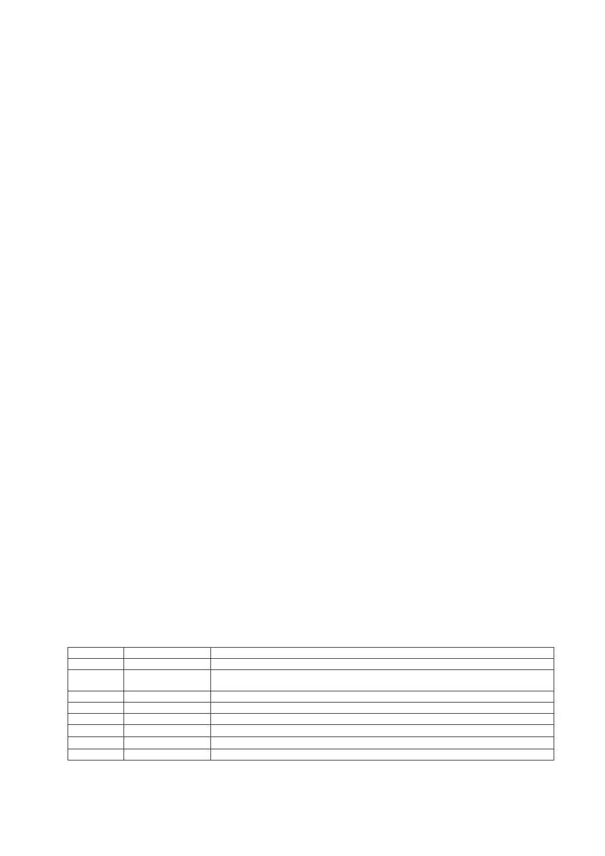
11.6.3. Pin Description
Symbol Pin name Functions
A
MS
1
-A
0
Address Inputs To provide memory addresses.
D
Q7
-D
Q0
Data Input/output To output data during Read cycles and receive input data during Program cycles.
The outputs are in tri-state when OE# or CE# is high.
CE# Chip Enable
To activate the device when CE# is low.
WE# Write Enable To program or erase (WE# = VIL pulse during Program or Erase)
OE# Output Enable To gate the data output buffers during Read operation when low
V
DD
Power Supply To provide 3.0V supply (2.7-3.6V)
V
SS
Ground
NC No Connection Unconnected pins.
1. A
MS
= Most significant address
A
MS
= A
15
for SST37VF512, A
16
for SST37VF010, A
17
for SST37VF020, and A
18
for SST37VF040
 Loading...