Do you have a question about the Icom IC-F5121D and is the answer not in the manual?
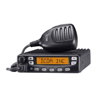
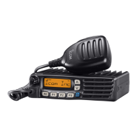
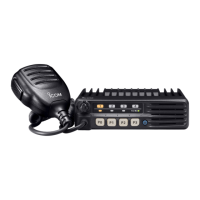
| Brand | Icom |
|---|---|
| Model | IC-F5121D |
| Category | Transceiver |
| Language | English |
Details frequency range, channel spacing, emission types, operating temperature, and physical dimensions.
Covers output power, modulation methods, frequency deviation, stability, and spurious emissions.
Details receiver sensitivity, squelch, selectivity, intermodulation, and audio output parameters.
Identifies key components on the front unit PCB, including CPU, EEPROM, and LCD driver.
Visually maps component placement on the top side of the main unit's printed circuit board.
Visually maps component placement on the bottom side of the main unit's printed circuit board.
Explains the RF, 1st IF, and 2nd IF/demodulator circuits for the receiver section.
Details the TX AF circuits, including modulation signal paths for analog and digital modes.
Describes the RX and TX VCO, PLL IC, and the reference frequency generation.
Illustrates voltage distribution across the transceiver's main circuit blocks.
Lists and describes the function of the CPU and D/A converter ports for interface.
Lists necessary equipment and their specifications required for performing calibration procedures.
Details procedures for adjusting PLL lock voltage and reference frequency using the utility.
Guides through adjusting TX power, modulation balance, and FM/digital deviation for optimal performance.
Outlines procedures for adjusting RX sensitivity, S-meter levels, and squelch threshold.
Visual representation of component placement on the top side of the front unit's PCB.
Visual representation of component placement on the bottom side of the front unit's PCB.
Visual representation of component placement on the top side of the main unit's PCB.
Visual representation of component placement on the bottom side of the main unit's PCB.
Shows voltage lines and their distribution across the front unit's electrical circuitry.
Details voltage lines and their distribution within the first section of the main unit's circuitry.
Details voltage lines and their distribution within the second section of the main unit's circuitry.
Details voltage lines and their distribution within the third section of the main unit's circuitry.