24
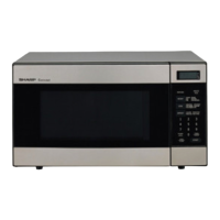
R-319FW
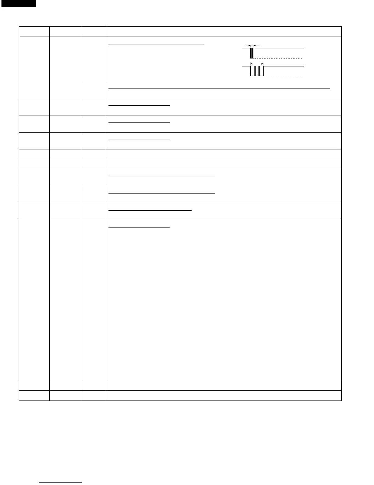
49 P36 OUT Signal to sound buzzer (2.0 kHz).
A: key touch sound.
B: Completion sound.
50 P37 IN To input signal which communicates the door open/close information to LSI.
Door close “H” level signal (0V). Door open “L” level signal (-5V).
51 COM0 OUT Common data signal.
Connected to LCD signal COM2.
52 COM1 OUT Common data signal.
Connected to LCD signal COM1.
53 COM2 OUT Common data signal.
Connected to LCD signal COM0.
54 COM3 OUT Terminal not used.
55 BIAS IN Power source voltage : GND(0V).
56 VLC0 IN Power source voltage input terminal.
Standard voltage for LCD. Connected to GND.
57-58
VLC1-VLC2
IN Power source voltage input terminal.
Standard voltage for LCD.
59 VSS0 IN Power source voltage: -5.0V.
The power source voltage to the LSI is input to VSS0 terminal. Connected toVC.
60-95 S0-S35 OUT Segment data signal.
Connected to LCD.
The relation between signals are as follows:
LSI signal (Pin No.) LCD (Pin No.) LSI signal (Pin No.) LCD (Pin No.)
S0 (60)
......................................
SEG 0 S18 (78)
....................................
SEG 18
S1 (61)
......................................
SEG 1 S19 (79)
....................................
SEG 19
S2 (62)
......................................
SEG 2 S20 (80)
....................................
SEG 20
S3 (63)
......................................
SEG 3 S21 (81)
....................................
SEG 21
S4 (64)
......................................
SEG 4 S22 (82)
....................................
SEG 22
S5 (65)
......................................
SEG 5 S23 (83)
....................................
SEG 23
S6 (66)
......................................
SEG 6 S24 (84)
....................................
SEG 24
S7 (67)
......................................
SEG 7 S25 (85)
....................................
SEG 25
S8 (68)
......................................
SEG 8 S26 (86)
....................................
SEG 26
S9 (69)
......................................
SEG 9 S27 (87)
....................................
SEG 27
S10 (70)
.....................................
SEG 10 S28 (88)
....................................
SEG 28
S11 (71)
.....................................
SEG 11 S29 (89)
....................................
SEG 29
S12 (72)
.....................................
SEG 12 S30 (90)
....................................
SEG 30
S13 (73)
.....................................
SEG 13 S31 (91)
....................................
SEG 31
S14 (74)
.....................................
SEG 14 S32 (92)
....................................
SEG 32
S15 (75)
.....................................
SEG 15 S33 (93)
....................................
SEG 33
S16 (76)
.....................................
SEG 16 S34 (94)
....................................
SEG 34
S17 (77)
.....................................
SEG 17 S35 (95)
....................................
SEG 35
96-99 P83-P80 OUT Terminal not used.
100 P25 OUT Terminal not used.
Pin No. Signal I/O Description
A
B
0.1 sec.
2.0 sec.
H : GND
L : -5V
H : GND
L : -5V
 Loading...