R-450C
15
LSI(IZA969DR)
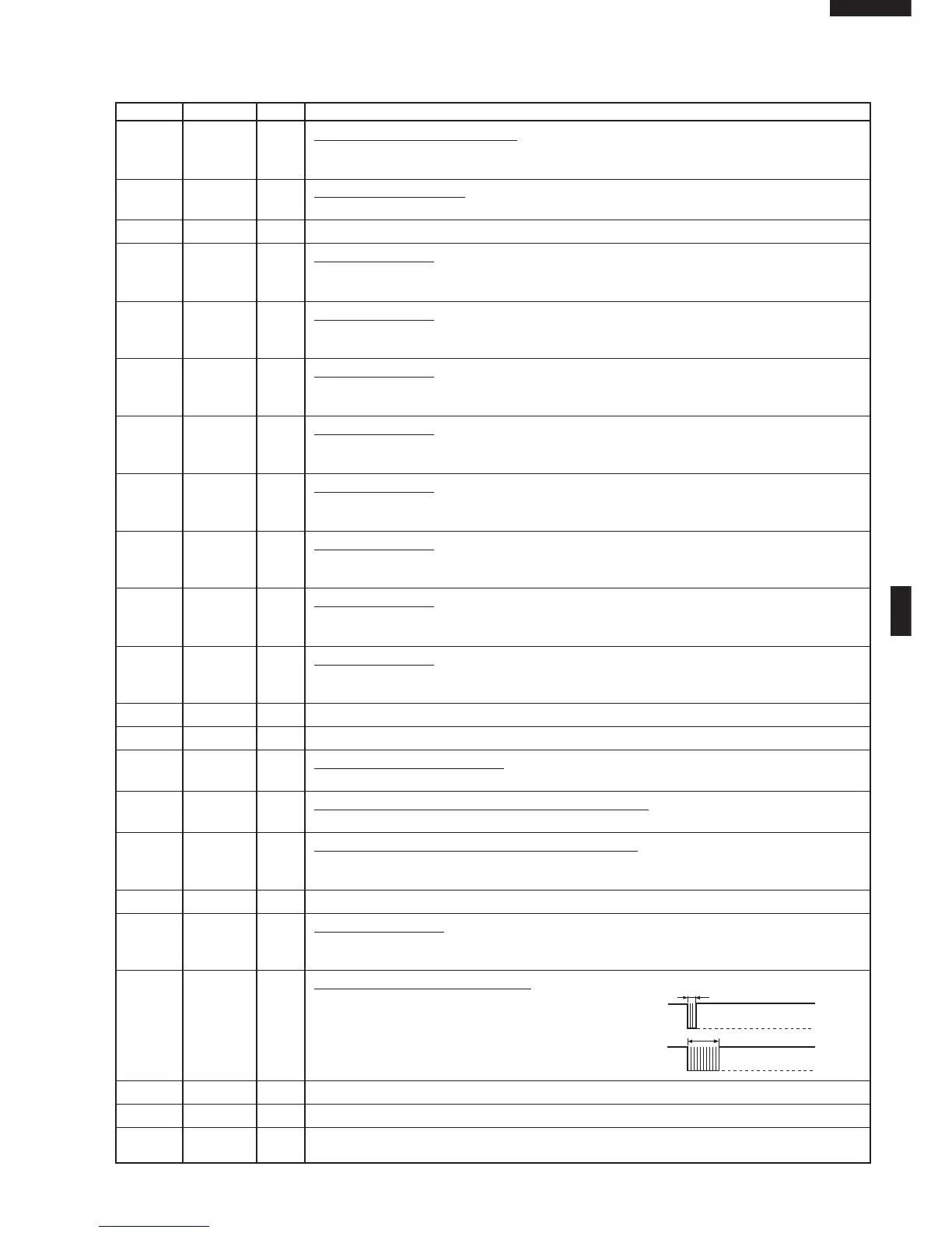
The I/O signal of the LSI(IZA969DR) is detailed in the following table.
Pin No. Signal I/O Description
1 AN10 IN
Signal coming from touch key.
When either G10 line on key matrix is touched, a corresponding signal out of P10 - P17 will
be input into AN10. When no key is touched, the signal is held at "H" level.
2 AN11 IN
Signal similar to AN10.
When either G9 line on key matrix is touched, a corresponding signal will be input into AN11.
3 AVSS IN Connected to VC.
4 P10 OUT
Key strobe signal.
Signal applied to touch-key section. A pulse signal is input to AN9, AN10, AN11, P41 and
P42 terminal while one of G8 line keys on key matrix is touched.
5 P11 OUT
Key strobe signal.
Signal applied to touch-key section. A pulse signal is input to AN9, AN10, AN11, P41 and
P42 terminal while one of G7 line keys on key matrix is touched.
6 P12 OUT
Key strobe signal.
Signal applied to touch-key section. A pulse signal is input to AN9, AN10, AN11, P41 and
P42 terminal while one of G6 line keys on key matrix is touched.
7 P13 OUT
Key strobe signal.
Signal applied to touch-key section. A pulse signal is input to AN9, AN10, AN11, P41 and
P42 terminal while one of G5 line keys on key matrix is touched.
8 P14 OUT
Key strobe signal.
Signal applied to touch-key section. A pulse signal is input to AN9, AN10, AN11, P41 and
P42 terminal while one of G4 line keys on key matrix is touched.
9 P15 OUT
Key strobe signal.
Signal applied to touch-key section. A pulse signal is input to AN9, AN10, AN11, P41 and
P42 terminal while one of G3 line keys on key matrix is touched.
10 P16 OUT
Key strobe signal.
Signal applied to touch-key section. A pulse signal is input to AN8, AN9, AN10, AN11, P41
and P42 terminal while one of G2 line keys on key matrix is touched.
11 P17 OUT
Key strobe signal.
Signal applied to touch-key section. A pulse signal is input to AN9, AN10, AN11, P41 and
P42 terminal while one of G1 line keys on key matrix is touched.
12 X1 IN Connected to GND.
13 X2 OUT Terminal not used.
14 VSS IN
Power source voltage: -5.0V.
VC voltage of power source circuit input.
15 OSC2 OUT
Internal clock oscillation frequency control output.
Output to control oscillation input of OSC2.
16 OSC1 IN Internal clock oscillation frequency input setting.
The internal clock frequency is set by inserting the ceramic filter oscillation circuit with respect
to OSC1 terminal.
17 TEST IN Connected to VC.
18 RES IN
Auto clear terminal.
Signal is input to reset the LSI to the initial state when power is applied. Temporarily set "L"
level the moment power is applied, at this time the LSI is reset. Thereafter set at "H" level.
19 P20 OUT
Signal to sound buzzer (2.0 kHz).
A: key touch sound.
B: Completion sound.
20 P21 OUT Terminal not used.
21 P22
IN/OUT
Terminal not used.
22 P23 OUT Terminal not used.
A
B
0.12 sec.
2.4 sec.
H : GND
L : -5V
H : GND
L : -5V
 Loading...