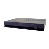
HBD-E280/T28
HBD-E280/T28
3333
For Schematic Diagrams.
Note:
• All capacitors are in μF unless otherwise noted. (p: pF) 50
WV or less are not indicated except for electrolytics and
tantalums.
• All resistors are in Ω and 1/4 W or less unless otherwise
specifi ed.
•
f
: internal component.
• C : panel designation.
THIS NOTE IS COMMON FOR PRINTED WIRING BOARDS AND SCHEMATIC DIAGRAMS.
(In addition to this, the necessary note is printed in each block.)
• A : B+ Line.
• B : B– Line.
• Voltages and waveforms are dc with respect to ground
under no-signal conditions.
no mark
: TUNER
*
: Impossible to measure
• Voltages are taken with VOM (Input impedance 10 MΩ).
Voltage variations may be noted due to normal production
tolerances.
• Waveforms are taken with a oscilloscope.
Voltage variations may be noted due to normal production
tolerances.
• Circled numbers refer to waveforms.
• Signal path.
F : AUDIO
E : VIDEO
J : DISC PLAY
L : USB
d : LAN
f : TUNER
• Abbreviation
AUS : Australian model
CND : Canadian model
IT : Italian model
MX : Mexican model
• The voltage and waveform of CSP (chip size package)
cannot be measured, because its lead layout is different
from that of conventional IC.
For Printed Wiring Boards.
Note:
• X : Parts extracted from the component side.
• Y : Parts extracted from the conductor side.
•
f
: Internal component.
• : Pattern from the side which enables seeing.
(The other layers' patterns are not indicated.)
• Indication of transistor.
C
B
These are omitted.
E
Q
B
These are omitted.
CE
Q
• Lead layouts
surface
CSP (Chip Size Package) Lead layout of conventional IC
Caution:
Pattern face side:
(Conductor Side)
Parts face side:
(Component Side)
Parts on the pattern face side seen
from the pattern face are indicated.
Parts on the parts face side seen from
the parts face are indicated.
• MB-141 board is multi-layer printed board. However, the
patterns of intermediate-layers have not been included in
this diagrams.
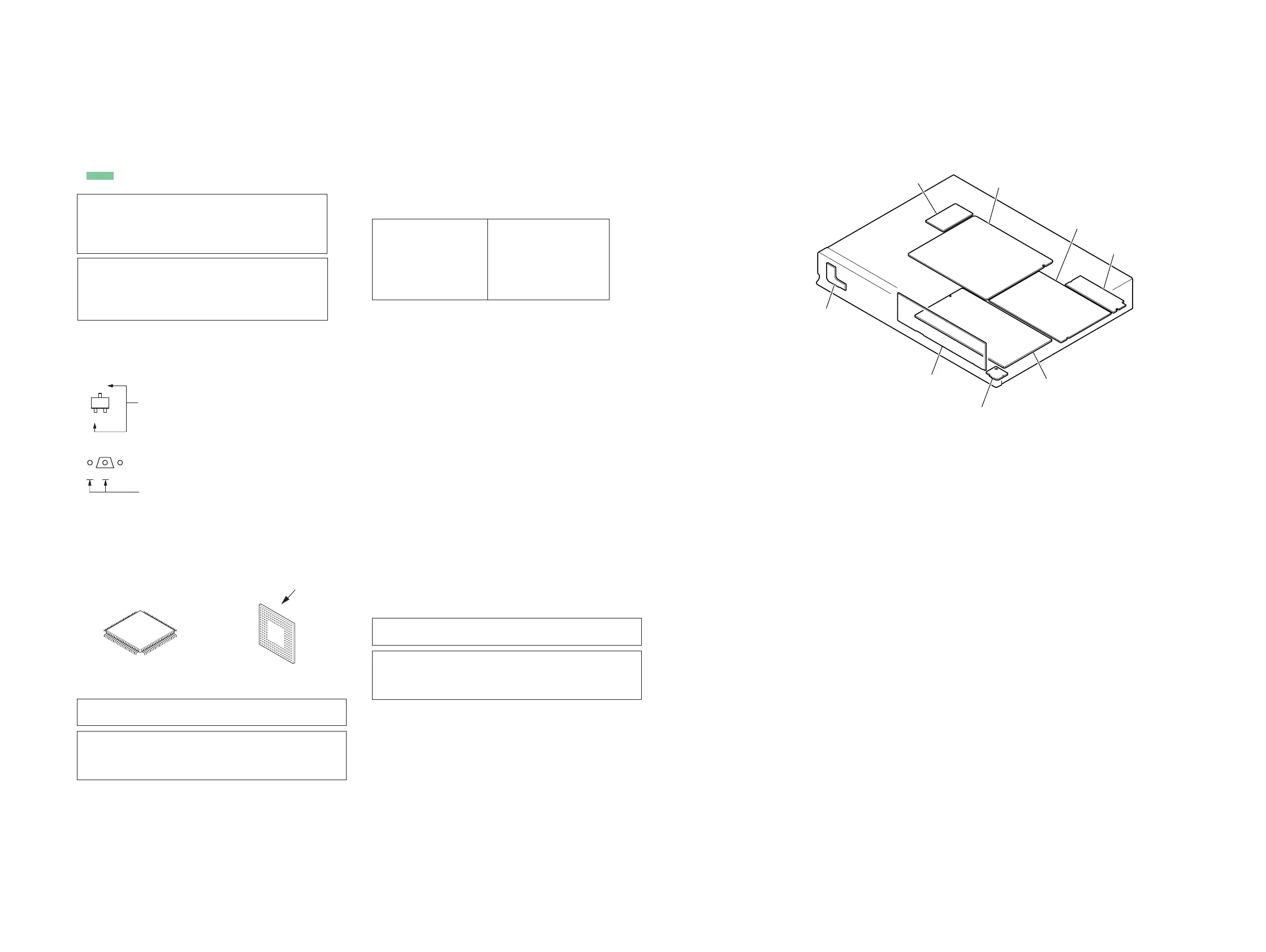
• Circuit Boards Location
Caution:
Pattern face side:
(SIDE B)
Parts face side:
(SIDE A)
Parts on the pattern face side seen
from the pattern face are indicated.
Parts on the parts face side seen from
the parts face are indicated.
Note:
The components identi-
fi ed by mark 0 or dotted
line with mark 0 are criti-
cal for safety.
Replace only with part
number specifi ed.
Note:
Les composants identifi és
par une marque 0 sont
critiques pour la sécurité.
Ne les remplacer que par
une pièce portant le nu-
méro spécifi é.
* Replacement of IC106, IC107, IC206, IC207 on the MB-141 board
used in this unit requires a special tool.
Note: When the AMP board is replaced, spread the compound refer-
ring to “NOTE OF REPLACING THE IC3100, IC3200 AND
IC3300 ON THE AMP BOARD AND THE COMPLETE AMP
BOARD” on servicing notes (page 9).
Note: When the AMP board is replaced, spread the compound refer-
ring to “NOTE OF REPLACING THE IC3100, IC3200 AND
IC3300 ON THE AMP BOARD AND THE COMPLETE AMP
BOARD” on servicing notes (page 9).
* Replacement of IC106, IC107, IC206, IC207 on the MB-141 board
used in this unit requires a special tool.
POWER KEY board
TUNER board
DISPLAY board
FRONT USB board
(AEP, IT, UK, AUS, MX)
SPEAKER board
AMP board
MB-141 board
switching regulator
(SWR1)
• Abbreviation
AUS : Australian model
CND : Canadian model
IT : Italian model
MX : Mexican model
Ver. 1.1
• Abbreviation
AUS : Australian model
IT : Italian model
MX : Mexican model
 Loading...