89
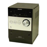
HCD-FX100W
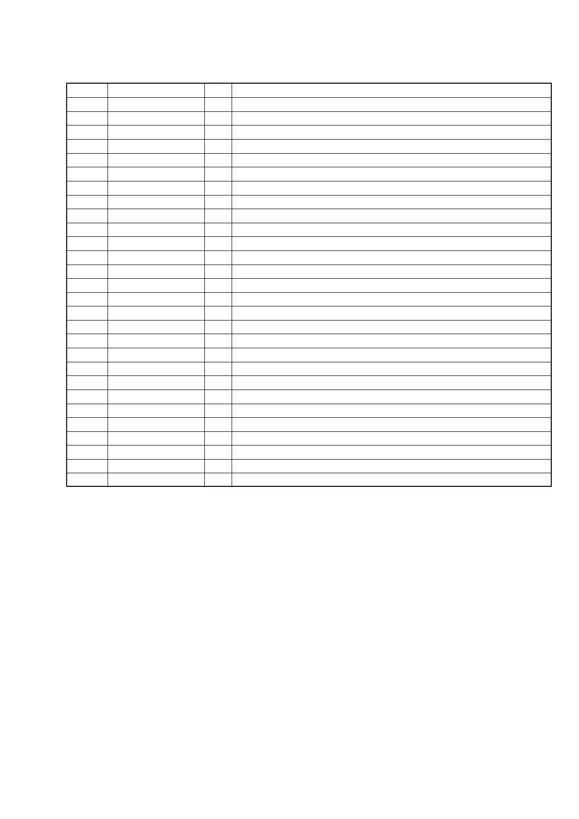
Pin No. Pin Name I/O Desciption
91 VSS — Digital ground
92 OVDDE2 — Digital positive supply voltage (+3.3V) for Pad Ring
93 to 95 QR7 to QR9 O R data output
96 QV O Vertical sync output
97 QH O Horizontal sync output
98 QDE O Data enable output
99 QCLK O Pixel clock output
100 VDDI — Digital positive supply voltage (+2.5V) for Pad Ring
101 VSS — Digital ground
102 EXCLK I Pixel clock input for external PLL mode.
103 OVDDE3 — Digital positive supply voltage (+3.3V) for Pad Ring
104 PH1 O Phase comparate signal-1 for external PLL (not used)
105 N.C — Not used
106 AVS1 — Analog ground for PLL
107 AVD1 — Digital positive supply voltage (+3.3V) for PLL
108 CPO O Charge pump output for internal PLL
109 N.C — Not used
110 VCI I VCO input for internal PLL
111 AVS2 — Analog ground for PLL
112 AVD2 — Digital positive supply voltage (+3.3V) for PLL
113 N.C — Not used
114 PH2 O Phase comparate signal-2 for external PLL (not used)
115 PLLEN I PLL mode select signal input (internal mode or external mode)
116 OVDDE4 — Digital positive supply voltage (+3.3V) for Pad Ring
117 DCLK I System clock input (27MHz)
118 OVSS1 — Digital ground
119 DCLKP I DCLK polarity control signal input
120 VDDI — Digital positive supply voltage (+2.5V) for Pad Ring
 Loading...