3/15
TDA7296
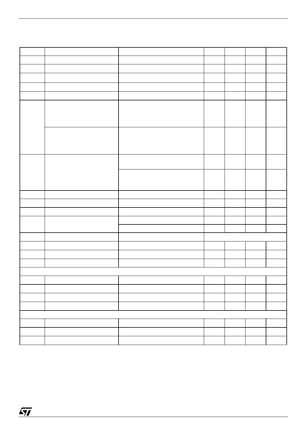
Table 4. Electrical Characteristcs (Refer to the Test Circuit V
S
= ±24V, R
L
= 8Ω, G
V
= 30dB; R
g
= 50Ω;
T
amb
= 25°C, f = 1 kHz; unless otherwise specified).
Note (*):
MUSIC POWER is the maximal power which the amplifier is capable of producing across the rated load resistance (regardless of non linearity)
1 sec after the application of a sinusoidal input signal of frequency 1KHz.
Note (**): Tested with optimized Application Board (see fig.5)
Symbol Parameter Test Condition Min. Typ. Max. Unit
V
S
Supply Range ±10 ±35 V
I
q
Quiescent Current 20 30 65 mA
I
b
Input Bias Current 500 nA
V
OS
Input Offset Voltage -10 10 mV
I
OS
Input Offset Current -100 100 nA
P
O
RMS Continuous Output
Power
d = 05%
V
S
= ± 24V, R
L
= 8Ω;
V
S
= ± 21V, R
L
= 6Ω;
V
S
= ± 18V, R
L
= 4Ω;
27
27
27
30
30
30
W
W
W
Music Power (RMS)
∆t = 1s (*)
d = 10%
V
S
= ± 29V, R
L
= 8Ω;
V
S
= ± 24V, R
L
= 6Ω;
V
S
= ± 22V, R
L
= 4Ω;
60
60
60
W
W
W
d Total Harmonic Distortion (**) P
O
= 5W; f = 1kHz
P
O
= 0.1 to 20W; f = 20Hz to 20kHz
0.005
0.1
%
V
S
= ± 18V, R
L
= 4Ω;
P
O
= 5W; f = 1kHz
P
O
= 0.1 to 20W; f = 20Hz to 20kHz
0.01
0.1
%
%
SR Slew Rate 7 10 V/µs
G
V
Open Loop Voltage Gain 80 dB
G
V
Closed Loop Voltage Gain (1) 24 30 40 dB
e
N
Total Input Noise A = curve 1 µV
f = 20Hz to 20kHz 2 5 µV
f
L ,
f
H
frequency response (-3dB) P
O
=1W 20Hz to 20kHz
R
i
Input Resistance 100 kΩ
SVR Supply Voltage Rejection f = 100Hz; V
ripple
= 0.5Vrms 60 75 dB
T
S
Thermal Shutdown 145 °C
STAND-BY FUNCTION (Ref: -Vs or GND)
V
ST on
Stand-by on Threshold 1.5 V
V
ST off
Stand-by off Threshold 3.5 V
ATT
st-by
Stand-by Attenuation 70 90 dB
I
q st-by
Quiescent Current @ Stand-by 1 3 mA
MUTE FUNCTION (Ref: -Vs ro GND)
V
Mon
Mute on Threshold 1.5 V
V
Moff
Mute off Threshold 3.5 V
AT T
mute
Mute AttenuatIon 60 80 dB
 Loading...