2232 Servlce
LIST OF ILLUSTRATIONS
3-l
3-2
3-3
3-4
3-5
37-6
3-7
3-8
3-9
6-1
6-2
6-3
6-4
6-5
6-6
6-7
9-l
9-2
9-3
9-4
9-5
9-6
9-7
9-8
9-9
9-10
9-11
9-12
9-13
9-14
9-15
9-16
9-17
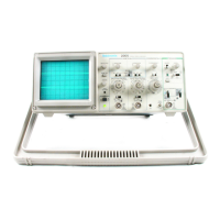
The2232Oscilloscope ...............................................
Maximum Input voltage versus frequency derating curve for the CW 1 OR X.
CH2ORY,andEXflNPUTconnectors ..................................
Physical dimensions of the 2232 Oscilloscope
............................
Securing the detachable power cord to the instrument
......................
Optional power cords. ................................................
Simplified block diagram ..............................................
Block diagram of the Channel 1 Attenuator circuit ..........................
Store/Non-Store Vertical Switching ......................................
Block Diagram of the Trigger Amplifiers and Switching
......................
A Sweep Generator and Logic circuitry
..................................
B Sweep Generator and Logic clrcultty ..................................
Horizontal Amplifier block diagram ......................................
Power Supply block dlagram ...........................................
Simplified diagram of the DC Restorer circuitry ............................
Multi-connector holder orientation ......................................
GroundingthesignallinesofP2111andP211.2 ...........................
Isolated Kernel timing .................................................
DiagnosticMenu Map ................................................
Location of screws and spacers on the Storage circuit board ................
Recessed screw and rear hinge removal .................................
Location of screws securing Power Supply shield and the support bracket to the
rearchassisframe ...................................................
Color codes for resistors and capacitors
Semiconductor lead configuratlons
Locating
COmpoflents
on schematic diagrams and circuit board illustrations
Detailed analog block diagram
Detailed storage block diagram
A2-Attenuator board
A14-CH 1 Logic board
A15-CH 2 Logic board
Al -Main board
Circuit View of Al -Main board
Al A8 - CH 1 Bandwidth Limit board
Al A9 - CH 2 Bandwidth Limit board
A3 - Front Panel board
Circuit view of A3 -
Front
Panel board
A4-Timing board
Al 3 -Sweep Interface board
A5-Alternate Sweep board
Page
VIII
I-17
1-18
2-l
2-2
-. 3-2
3-8
3-l 1
3-14
3-18
3-21
3-25
3-36
3-40
6-7
6-7
6-6
6-16
6-27
6-28
6-30
 Loading...