Circuit Description—475
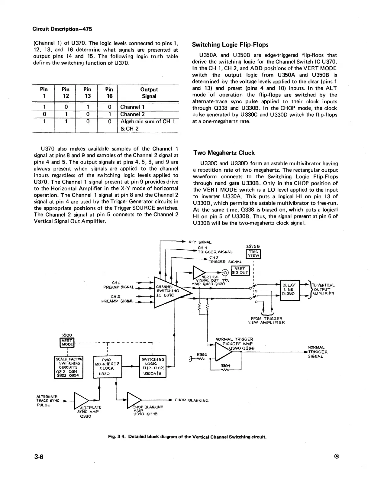
(Channel 1) of U370. The logic levels connected to pins 1,
12, 13, and 16 determine what signals are presented at
output pins 14 and 15. The following logic truth table
defines the switching function of U370.
Pin
Pin Pin Pin Output
1 12 13
16
Signal
1
0
1
0
Channel 1
0
1
0
1
Channel 2
1 1 0 0
Algebraic sum of CH 1
& CH 2
U370 also makes available samples of the Channel 1
signal at pins 8 and 9 and samples of the Channel 2 signal at
pins 4 and 5. The output signals at pins 4, 5, 8, and 9 are
always present when signals are applied to the channel
inputs regardless of the switching logic levels applied to
U370. The Channel 1 signal present at pin 9 provides drive
to the Horizontal Amplifier in the X-Y mode of horizontal
operation. The Channel 1 signal at pin 8 and the Channel 2
signal at pin 4 are used by the Trigger Generator circuits in
the appropriate positions of the Trigger SOURCE switches.
The Channel 2 signal at pin 5 connects to the Channel 2
Vertical Signal Out Amplifier.
Switching Logic Flip-Flops
U350A and U350B are edge-triggered flip-flops that
derive the switching logic for the Channel Switch 1C U370.
In the CH 1, CH 2, and ADD positions of the VERT MODE
switch the output logic from U350A and U350B is
determined by the voltage levels applied to the clear (pins 1
and 13) and preset (pins 4 and 10) inputs. In the ALT
mode of operation the flip-flops are switched by the
alternate-trace sync pulse applied to their clock inputs
through Q338 and U330B. In the CHOP mode, the clock
pulse generated by U330C and U330D switch the flip-flops
at a one-megahertz rate.
Two Megahertz Clock
U330C and U330D form an astable multivibrator having
a repetition rate of two megahertz. The rectangular output
waveform connects to the Switching Logic Flip-Flops
through nand gate U330B. Only in the CHOP position of
the VERT MODE switch is a LO level applied to the input
to inverter U330A. This puts a logical HI on pin 13 of
U330D, which permits the astable multivibrator to free-run.
At the same time, Q338 is biased on, which puts a logical
HI on pin 5 of U330B. Thus, the signal present at pin 6 of
U330B will be the two-megahertz clock signal.
CH X.
PREAMP SIGNAL
CH2
PREAMP SIGNAL
X-Y SIGNAL
CH 1
TRIGGER SIGNAL
CH 2
TRIGGER SIGNAL
S375B
TRIG
V IE W
H >
L X ve
— 'O l/iK I A
^ VERT
- O) SIG OUT
VERTICAL T
SIGNAL OUT
AMP Q420 Q430
S300
VERT I
MODE
T '
l
I
1
SCALE FACTOR
TWO
SWITCHING
SWITCHING
MEGAHERTZ
LOGIC
CIRCUITS
CLOCK
FLIP-FLOPS
Q3I2 Q3I4
0322 Q324
U330
U350A<|B
DELAY
LINE
DL380
J
-----------------
11
► \to VERTICAL
) OUTPUT
J AMPLIFIER
FROM TRIGGER
VIEW AMPLIFIER
NORMAL TRIGGER
PICKOFF AMP
Q390 Q336
NORMAL
►TRIGGER
SIGNAL
CHOP BLAN kING
CHOP BLANKING
AMP
U340 Q348
3-6
Fig. 3-4. Detailed block diagram of the Vertical Channel Switching circuit.
 Loading...


