2LV/2L1/2L2/2MS/2MT
2-3-12
YC20 B12 VDATA1P I LVDS Video data 1 signal (+)
Connected to
the main
PWB
B13 VDATA1N I LVDS Video data 1 signal (-)
B14 PLGCLK I 0/3.3 V DC (pulse) PM clock signal
B15 E2C_SDAT O 0/3.3 V DC (pulse) Serial communication data output
B16 C2E_SCKN I 0/3.3 V DC (pulse) Serial communication clock
B17 E2C_SDIR O 0/3.3 V DC Communication direction change signal
B18 VSYNC O 0/3.3 V DC (pulse) Sub scanning synchronizing signal
B19 C2E_OFFRD
Y
I 0/3.3 V DC Off-mode notice signal
B20 C2E_INT I 0/3.3 V DC Interrupt signal
YC21 1 TH2 I Analog FUTH2 output signal
Connected to
the fuser
thermistor
connect
PWB
2 TH1 I Analog FUTH1output signal
3 GND - - Ground
4 REARFANN O 24 V DC REFM: On/Off
5 +24V4 O 24 V DC 24 V DC power output to FTHPWB
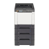
YC22 1 +24V5 O 24 V DC 24 V DC power output to PF
Connected to
the paper
feeder
2 OPSDO O 0/3.3 V DC (pulse) PF communication serial data signal
3 OPSDI I 0/3.3 V DC (pulse) PF communication serial data signal
4 OPCLK O 0/3.3 V DC (pulse) PF communication serial clock signal
5 OPRDYN I 0/3.3 V DC Option communication ready signal
6 +3.3V7 O 3.3 V DC 3.3 V DC power output to PF
7 GND - - Ground
8 OPSEL2 O 0/3.3 V DC PF select signal
9 OPSEL1 O 0/3.3 V DC PF select signal
10 OPSEL0 O 0/3.3 V DC PF select signal
11 OPPAUSEN O 0/3.3 V DC Paper stop signal
12 GND - - Ground
YC23 1 VBUS O 5 V DC 5 V DC power output to USB host
Connected to
the USB host
2 UDATAN I/O LVDS USB data signal (-)
3 UDATAP I/O LVDS USB data signal (+)
4 GND - - Ground
5 GND - - Ground
YC26 1 +3.3V13 O 3.3 V DC 3.3 V DC power output to ES
Connected to
the eject sen-
sor
2 GND - - Ground
3 EXITSENSN I 0/3.3 V DC ES: On/Off
Connector Pin Signal I/O Voltage Description
 Loading...