— 11 —
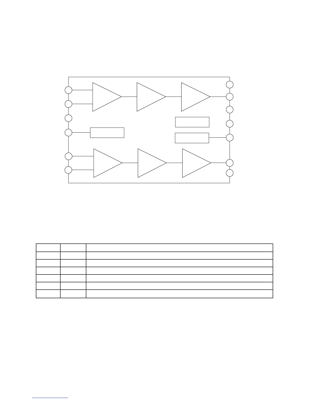
Power Amplifier (LA4598)
The power amplifier is a two-channel amplifier with standby switch. The following figure shows the inter-
nal diagram of the amplifier.
Internal Diagram of LA4598
6
5
8
7
10
11
13
12
9
4
1
3
2
Input
Amp.
Pre-drive
Amp.
Power
Amp.
TSD protector
Stand by
Bias circuit
Input
Amp.
Pre-drive
Amp.
Power
Amp.
Ch1 IN
Ch1 N.F.
Pre GND
D.C.
Ch2 IN
Ch2 N.F.
Ch2 B.S.
Ch1 OUT
Power GND
VCC
Standby
Ch2 OUT
Ch2 B.S.
Power Supply Circuit
The power supply circuit generates six voltages as shown in the following table. VDD voltage is always
generated. The others are controlled by APO signal output from the CPU.
Name Voltage For operation of
VDD +5 V CPU, Reset IC, Working strage RAM
DVDD +5 V DSP, Key controller, Sound source ROM, Effect RAM, DAC, KO siginal generator
AVDD +5 V DAC Filter
LVDD +4.5 V LED Driver
VCC +9 V Pilot lamp
VC +9 V Power amplifier
 Loading...