— 7 —
MEMORY DEVICES
Each memory device has the following data.
1 RAM1 :
S-RAM for operation program, Register, Pattern, Song
and SMF data from FDD. (Lower part of data bus)
2 RAM2 :
S-RAM for operation program, Register, Pattern, Song
and SMF data from FDD. (Upper part of data bus)
3 Internal ROM of CPU :
Main program data for system operation
4 Internal RAM of CPU :
Work area for system operation
5 ROM1 :
Demo, Accompaniment data, Song, Pattern, Synth, Disk
mode
6 ROM2 :
Sound Waveforms/Tone data Digital sound effect
7 Working RAM :
Work area for DSP
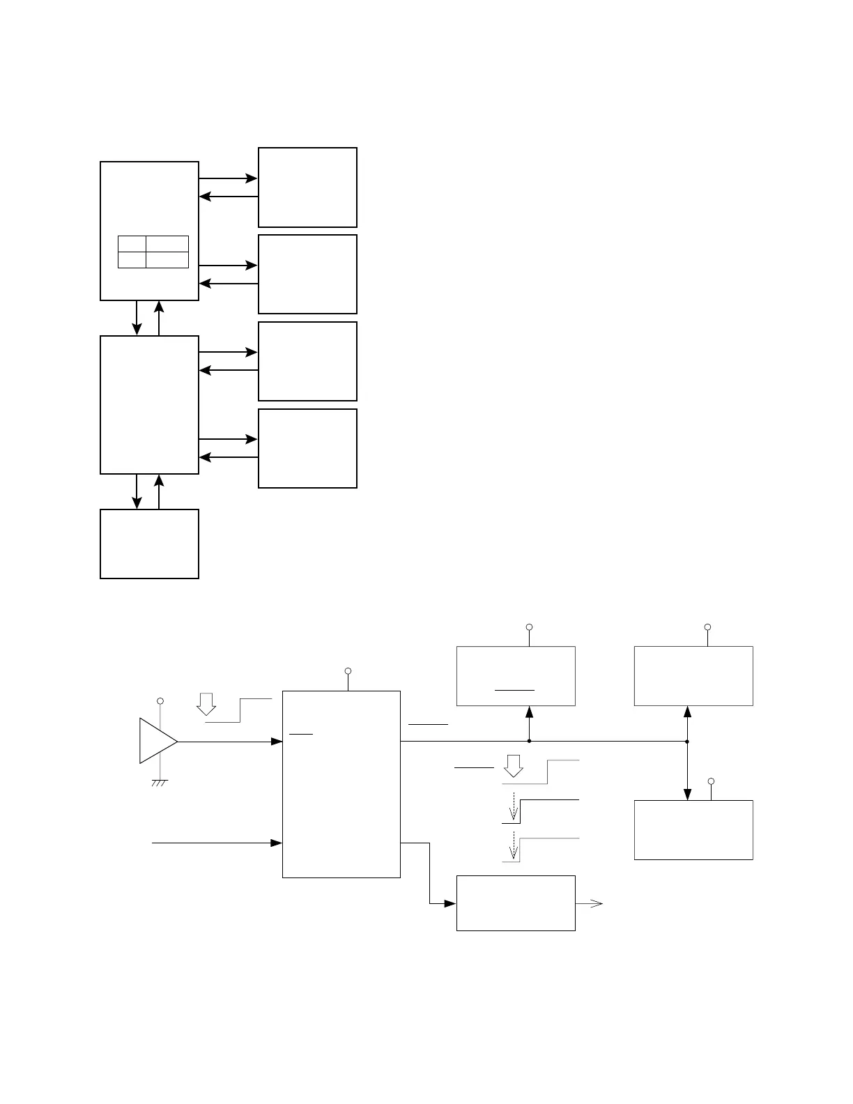
CPU
RAM1
1
1 Mbit
LSI7
ROM
RAM
3
4
512 kbit
16 kbit
DSP
LSI9
LSI4
Working RAM
7
256 kbit
LSI5
Internal Memory
ROM1
5
8 Mbit
LSI2
RAM2
2
1 Mbit
LSI8
ROM2
6
32 Mbit
LSI3
VDD
Battery set
RESET
CPU
HD6433042SB51F
LSI9
FDD Controller
HD63266F
LSI6
RESET
Power Supply
Circuit
DSP
HG51B155FD
LSI4
RESB
RESB
Key Controller
TC190C020AF-001
LSI10
DVDD
DVDD
DVDD
VDD
DVDD
RESET
APO
PWSW
From power switch
RES
NMI
PB0
PA7
RESET
PW/SW ON
APO
DVDD
(5V)
Initial reset
When batteries are set or an AC adapter is connected, the reset IC provides a low pulse to the CPU.
When the power switch is pressed, the CPU receives a low pulse of POWER signal. The CPU first raises
APO signal to +5 V to generate DVDD voltage, then raises RESET signal to +5 V. During this period the
DSP, the key controller and FDD controller LSIs initialize their internal circuits.
RESET CIRCUIT
 Loading...