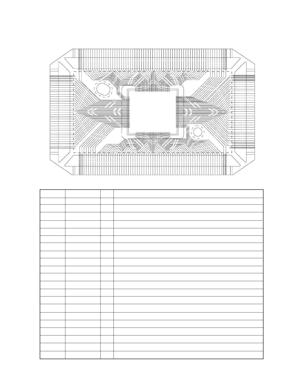
— 12 —
Pin No. Signal I/O Function
1 ~ 5 C0 ~ 4 Out Common Signal for display
6 GND In GND /0[V]
7,8 BZ1,2 Out Buzzer terminal
9 VDD In Power supply/5.3[V]
10 CSRA1 Out Chip enable signal (Not used)
11 CSRA2 Out Chip enable signal for RAM
12 CSROM Out Chip enable signal (Not used)
13 WEB Out Write enable signal for RAM
14,15 RA15,16 Out Address bus (Not used)
16 ~ 30 A0 ~ 14 Out Address bus
31 ~ 38 IO0 ~ 7 I/O Data bus
39 ~ 54 KY0 ~ 15 I/O Key signal
55 SW In Battery switch (On: "L"/0[V] Off: "H"/6[V])
56 DEBUG - Test for manufacturer
57 ON Out Data communication enable
58 CRCKI In GND/0[V]
59 SOUTB Out Transmission data output
60 SIN In Transmission data input
61 VDD In Power supply/5.3[V]
62 TEST - Test for manufacturer
63 VTM - Not used
6. LSI, IC (Pin function)
6-1. CPU
No.1
“
 Loading...