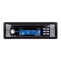
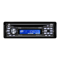
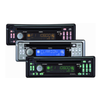
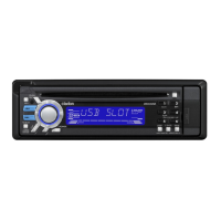
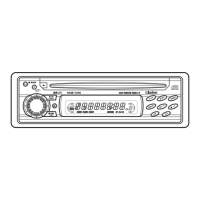
DB345MP/DB346MPDB345MP/DB346MP
DB345MP/DB346MPDB345MP/DB346MP
DB345MP/DB346MP
- 8 -- 8 -
- 8 -- 8 -
- 8 -
1 RESET I Reset Port
2 MiMD I Mode selection (H:I²C L:Serial)
3 MiCS I NC
4 MiLP I NC
5 MiDio I/O Data input and output for
micom Interface (I²C:SDA)
6 MiCK I Clock input for micom interface
(I²C:SCL)
7 MiACK O NC
8 VDDT - VDD 3.3V
9 SDo O Data output
10 BCKo O NC
11 LRCKo O NC
12 SDi0 I Data Input-0
13 BCKiA I Bit Clock Input-A
14 LRCKiA I LR Clock Input-A
15 SDi1 I NC
16 BCKiB I NC
17 LRCKiB I NC
18 VDD - VDD 2.5V
19 STANDBY I Control input for Stand-by
mode (H:STBY L:Normal)
20 VSS - GND
21 VSSL - GND
22 VRAL - NC
23 LO O NC
24 VDAL - VDD 2.5V
25 VDAR - VDD 2.5V
26 RO O NC
27 VRAR - NC
28 VSSR - GND
29 TESTP I GND
30 TXO O NC
31 Po0 O NC
32 Po1 O NC
33 Po2 O NC
34 Po3 O NC
35 VDDT - VDD 3.3V
36 Po4 O NC
37 Po5 O NC
38 Po6 O NC
39 Po7 O Request pin for interrupt host
40 VSS - GND
41 REQ I/O NC
42 VDDM - VDD 2.5V
43 Fi0 I NC
44 Fi1 I NC
45 VSSM - GND
46 Pi0 I NC
47 Pi1 I NC
48 VSS - GND
49 Pi2 I NC
50 Pi3 I NC
51 Pi4 I NC
52 VDD - VDD 2.5V
53 Pi5 O NC
54 TSTiN I NC
55 Fi2 I NC
56 VSSP - GND
57 Pdo O Phase detector output
58 Vcoi I Controlled voltage input for VCO
circuit
59 VDDP - VDD 2.5V
60 CKi I/O NC
61 VDDX - VDD 2.5V
62 Xi I X-TAL 16.9344MHz
63 Xo O X-TAL 16.9344MHz
64 VSSX - GND
77 RO O Right channel data output for 1-bit
DAC.
78 D VDD - Positive supply voltage for the
digital section.
79 D Vref O Digital reference voltage.
80 LO O Left channel data output for 1-bit
DAC.
81 D VSS - Digital ground.
82 Z DET O O 1bit DAC zero flag output.
83 VSS - Negative supply voltage.
84 BUS 0 I/O CD IC Data input / output.
85 BUS 1 I/O CD IC Data input / output.
86 BUS 2 I/O CD IC Data input / output.
87 BUS 3 I/O CD IC Data input / output.
88 BU CK IN I CD IC Data clock input.
89 CCEI I Chip enable input.
Pin No PIN NAME I/O DESCRIPTIONPin No PIN NAME I/O DESCRIPTION
90 RSTI I Reset signal input.
91 VDD - Positive supply voltage.
92 EMPHI/FAO I/O Emphasis input for 1-bit DAC /
Flag A output.
93 BCKI/FBO I/O Bit clock input for 1-bit DAC / Flag
B output.
94 AIN/FCO I/O Audio input for 1-bit DAC / Flag C
output.
95 LRCKI/FDO I/O LR clock input for 1-bit DAC /
Flag D output.
96 EMPHO O Emphasis flag output.
H=Emphasis ON.
97 B CK O O Bit clock output.
98 A OUT O Audio signal output.
99 LR CK O O LR clock output.
100 D OUT O Serial data output.
TC94A20F 051-6704-00
MP3 Decorder IC
Outward FormOutward Form
Outward FormOutward Form
Outward Form
64 pins, plastic QFP
Terminal Description
Pin No PIN NAME I/O DESCRIPTIONPin No PIN NAME I/O DESCRIPTION
 Loading...