CP-650 Service Manual
DTV R&D Europe
32
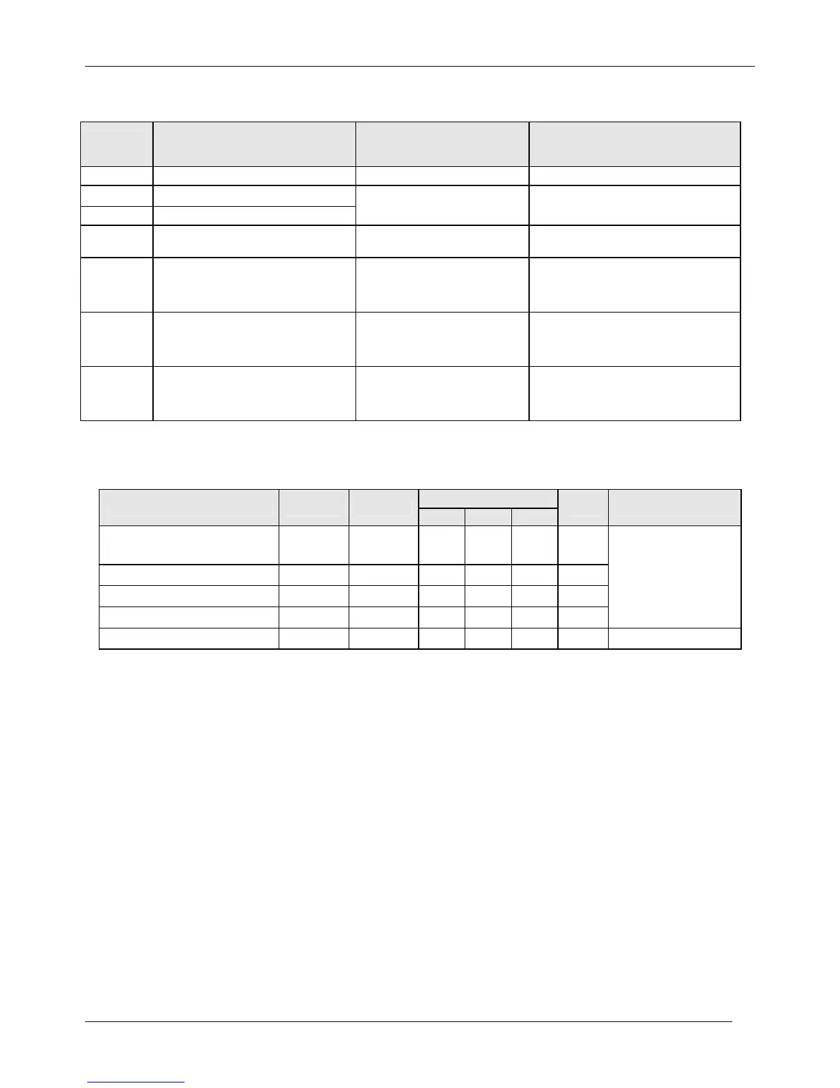
4.6.4 PIN DESCRIPTION
4.6.5 MOSFET ELECTRICAL CHARACTERISTICS
Ratings
Parameters Terminal Symbols
M I N T Y P M A X
Units Conditions
Drain-Source Voltage ※
7
1 - 3 VDSS 650 ― ― V
Drain Leakage Current 1 - 3 IDSS
― ―
300 µA
ON Resistance ※7
1 - 3 RDS(ON)
― ―
0.73
Ω
Switching Time 1 - 3
tf ― ―
Nsec
※6
Thermal Resistance ※7 ― θ ch-F ― ―
℃/W
Channel – Internal Frame
Pin No. Symbols
Terminal
Descriptions
Functions
1 D Drain Terminal MOSFET Drain
2
-
3 S/GND
Source/Grand
Terminal
MOSFET Source and
Ground
4 VCC
Power Supply Terminal
Control Circuit Power Supply
Input
5 SS/OLP
Delay at Overload/Soft-
Start set up Terminal
Overload Protection and
Soft- Start Operation Time
set up
6 FB Feedback Terminal
Constant Voltage Control
Signal Input, Blocking
Oscillation Control
7 OCP/BD
Overcurrent Protection
Input/Bottom Detection
Terminal
Overcurrent Detection
Signal Input / Bottom
Detection Signal Input
 Loading...