46
46
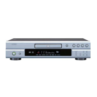
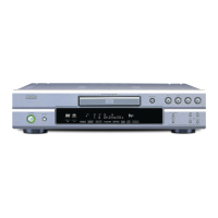
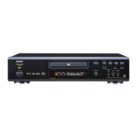
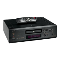
DVD-2900
50 TESTO O Output for TEST. (open)
51 TESTI I Input for TEST. It fixed to “L” potential.
52 TESTI I Input for TEST. It fixed to “L” potential.
53 TESTO O Output for TEST. (open)
54 VDC - +2.5V Power for CORE.
55 DSADML O DSD Data output terminal for Lch Down Mix.
56 DSADMR O DSD Data output terminal for Rch Down Mix.
57 BCKASL I I/O selection terminal of the Bit clock for DSD data output. L=input (Slave), H=output (Master)
58 VSDSD - Ground terminal for DSD data output.
59 BCKAI I Bit clock input terminal for DSD data output.
Input a Bit clock into this terminal at the time of BCKASL=”L” potential.
60 BCKAO O Bit clock output terminal for DSD data output.
Bit clock output from this terminal at the time of BCKASL=”H” potential.
61 PHREFI I Reference phase signal input terminal for DSD output phase modulation.
62 PHREFO O Reference phase signal output terminal for DSD output phase modulation.
63 ZDFL O Lch zero-data detection flag (at the time of µcom setup).
It will be set to “H” if non-sound data continues 300 msecs.
64 DSAL O DSD data output terminal for Lch speaker.
65 ZDFR O Rch zero-data detection flag (at the time of µcom setup).
It will be set to “H” if non-sound data continues 300 msecs.
66 DSAR O DSD data output terminal for Rch speaker.
67 V
DD
SD - +3.3V Power for DSD data output.
68 ZDFC O Cch zero-data detection flag (at the time of µcom setup).
It will be set to “H” if non-sound data continues 300 msecs.
69 DSAC O DSD data output terminal for Cch speaker.
70 ZDFLFE O LFEch zero-data detection flag (at the time of µcom setup).
It will be set to “H” if non-sound data continues 300 msecs.
71 DSASW O DSD data output terminal for SWch speaker.
72 VSDSD - Ground for DSD data output.
73 ZDFLS O LSch zero-data detection flag (at the time of µcom setup).
It will be set to “H” if non-sound data continues 300 msecs.
74 DSALS O DSD data output terminal for LSch speaker.
75 ZDFRS O RSch zero-data detection flag (at the time of µcom setup).
It will be set to “H” if non-sound data continues 300 msecs.
76 DSARS O DSD data output terminal for RSch speaker.
77 V
DD
SD O +3.3V Power for DSD data output.
78 IOUT0 O Data output terminal 0 for IEEE1394 link chip I/F.
79 IOUT1 O Data output terminal 1 for IEEE1394 link chip I/F.
80 VSC - Ground for CORE.
81 IOUT2 O Data output terminal 2 for IEEE1394 link chip I/F.
82 IOUT3 O Data output terminal 3 for IEEE1394 link chip I/F.
83 VDC - +2.5V Power for CORE.
84 IOUT4 O Data output terminal 4 for IEEE1394 link chip I/F.
85 IOUT5 O Data output terminal 5 for IEEE1394 link chip I/F.
86 VSIO - Ground for I/O.
87 IANCO O Transmission information data output terminal for IEEE1394 link chip I/F.
88 IFULL I Data transmission hold request signal input terminal for IEEE1394 link chip I/F.
89 IEMPTY I High speed transmission request signal input terminal for IEEE1394 link chip I/F.
90 VDIO - +3.3V Power for I/O.
91 IFRM O Frame reference signal output terminal for IEEE1394 link chip I/F.
92 IOUTE O Enable signal output terminal for IEEE1394 link chip I/F.
93 IBCK O Data transmission clock output terminal for IEEE1394 link chip I/F.
94 VSC - Ground for CORE.
95 TESTI I TEST input terminal. It fixed to “H” potential.
Pin Name I/O Functions
w
w
w
.
x
i
a
o
y
u
1
6
3
.
c
o
m
Q
Q
3
7
6
3
1
5
1
5
0
9
9
2
8
9
4
2
9
8
T
E
L
1
3
9
4
2
2
9
6
5
1
3
9
9
2
8
9
4
2
9
8
0
5
1
5
1
3
6
7
3
Q
Q
TEL 13942296513 QQ 376315150 892498299
TEL 13942296513 QQ 376315150 892498299
http://www.xiaoyu163.com
http://www.xiaoyu163.com
 Loading...