67
67
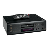
DVD-2900
Terminal Function
PIN
I/O
DSDL 1 I/O L-channel audio data input for DSD and external DF modes
‡
PCM mode zero flag for L-channel by ZERO output mode select
DSDR 2 I/O R-channel audio data input for DSD and external DF modes
‡
PCM mode zero flag for R-channel by ZERO output mode select
DBCK 3 I Bit clock input for external DF and DSD modes
†
PLRCK 4 I Left and right clock (f
S
) input for normal operation. WDCK clock input for external DF mode.
Connected to GND for DSD mode
†
PDATA 5 I Serial audio data input for normal operation
†
TERMINAL
NAME
DESCRIPTIONS
DGND 8 - Digital ground
V
DD
9 - Digital pow
er supply, +3.3 V
MS
10 I/O Chip select for mode control
‡
MDI 11 I Mode control data input
†
MC 12 I Mode control clock input
†
MDO 13 I/O Mode control read back data output
‡
RST
14 I Reset
†
V
CC
2R 15 - Analog power supply (R-channel DACFF), +5.0 V
AGND3R 16 - Analog ground (R-channel DACFF)
I
OUT
R+ 17 O R-channel analog current output +
I
OUT
R– 18 O R-channel analog current output –
AGND1 19 - Analog ground (internal bias)
I
REF
20 - Output current reference bias pin
V
COM
R 21 - R-channel Internal bias de-coupling pin
V
COM
L 22 - R-channel Internal bias de-coupling pin
V
CC
1 23 - Analog power supply, +5.0 V
AGND2 24 - Analog ground (internal bias)
I
OUT
L+ 25 O L-channel analog current output +
I
OUT
L– 26 O L-channel analog current output –
AGND3L 27 - Analog ground (L-channel DACFF)
V
CC
2L 28 - Analog power supply (L-channel DACFF), +5.0 V
† Schmitt trigger input, 5 V tolerant.
‡ Schmitt trigger input and output, 3.3 V.
PBCK 6 I Bit clock input. Connected GND for DSD mode
†
SCK 7 I System clock input
†
w
w
w
.
x
i
a
o
y
u
1
6
3
.
c
o
m
Q
Q
3
7
6
3
1
5
1
5
0
9
9
2
8
9
4
2
9
8
T
E
L
1
3
9
4
2
2
9
6
5
1
3
9
9
2
8
9
4
2
9
8
0
5
1
5
1
3
6
7
3
Q
Q
TEL 13942296513 QQ 376315150 892498299
TEL 13942296513 QQ 376315150 892498299
http://www.xiaoyu163.com
http://www.xiaoyu163.com
 Loading...