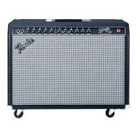
STAGE® 100/160 DSP
(This is the model name for warranty claims)
5
CIRCUIT DESCRIPTION
This section provides an overview of any new or
unusual circuitry incorporated into this amplifier
model. The purpose is to aid the service technician
by providing insight into the design areas most
likely to present a challenge in troubleshooting.
This overview is focused for the efficient use and
security of Fender® proprietary information.
PRE-AMPLIFIER
The guitar input signal is fed into the high pass filter
at U1–A before splitting into two signal paths. The
normal channel signal path (U1–B to U3–B) is ac-
tive until FETs Q2, Q4, and Q6 are turned on
activating the drive channel signal path (U2–A to
U3–B). Turning on FETs Q1, Q3, and Q5 activates
the “More Drive” channel signal path for increased
gain and sustain. Differential amp U8–A and fol-
lower U8–B adjust the signal level and provides
+1.65VDC bias voltage to the uDSP effects card.
The preamp is in series with the digital effects card,
therefore, disconnecting the card breaks the overall
signal path. The low pass filter at U5–B recovers
the signal from the uDSP card and sends it to the
external effects loop and power amplifier.
POWER AMPLIFIER
“Flying Rail” power amp topology. The output stage
is referenced to ground, and the output signal is de-
rived from the center tap of the high voltage power
supply (C86 & C87) which is floating. Diff–amp U7–
B amplifies voltage developed at the load sense re-
sistors (R120–123) to provide negative current
feedback. Inserting an 8Ω load at Ext. Spkr (J7)
turns on FET Q20 creating an attenuation network
(R117–119) to compensate for the increased cur-
rent at 4Ω total load impedance. This allows the
amplifier to have a similar frequency response run-
ning either an 8 or 4Ω speaker load.
Thermistor RT2 monitors the heatsink temperature.
Its resistance increases with temperature and at
approx. 100 ºC turns on xstr Q23. This shorts out
C77, turning on FET Q22 providing a muting func-
tion at the power amp input. The amplifier remains
muted until the heatsink cools down, at which point,
normal operation is restored.
POWER SUPPLY
Standard bridge rectifiers for both high and low
voltage sections, with zener regulation (D52–53) for
the +/–16V supplies. Half–wave rectifier (D46–47,
C48) supplies U11, 7805 regulator for +5V supply
for the uDSP card and digital user–interface.
DIGITAL USER INTERFACE
The uDSP effects card generates clock signals HD0
(~45Hz) and HD1 (~90Hz) which control the 4053
CMOS switch to read pots R134, R135, and R138.
The DC level (0–5V) of the pots controls the reverb
level, fx level, and fx time/rate. Power (+3.3V) is
switched to encoders S4 and S5 via the 4053, also
controlled by HD0. The outputs of the 4–bit encod-
ers, isolated by diodes D28–D35, determine the
active reverb and fx algorithms (HD4–HD7).
DIGITAL NOISE
The uDSP effects card generates some high fre-
quency noise (>50kHz), which is a normal product
of DSP processing. This noise is not audible and
does not effect amplifier performance, but may be
visible when observing the output of the amplifier on
an oscilloscope.
.
 Loading...