4-2
S40889-01
CIRCUIT BOARD NOTES
1. Foil and Component sides
1) Foil side (B side) :
Parts on the foil side seen from foil face (pattern face)
are indicated.
2) Component side (A side) :
Parts on the component side seen from component face
(parts face) indicated.
2. Parts location guides
Parts location are indicated by guide scale on the circuit board.
Note: For general information in service manual, please
refer to the Service Manual of GENERAL INFORMA-
TION Edition 4 No. 82054D (January 1994).
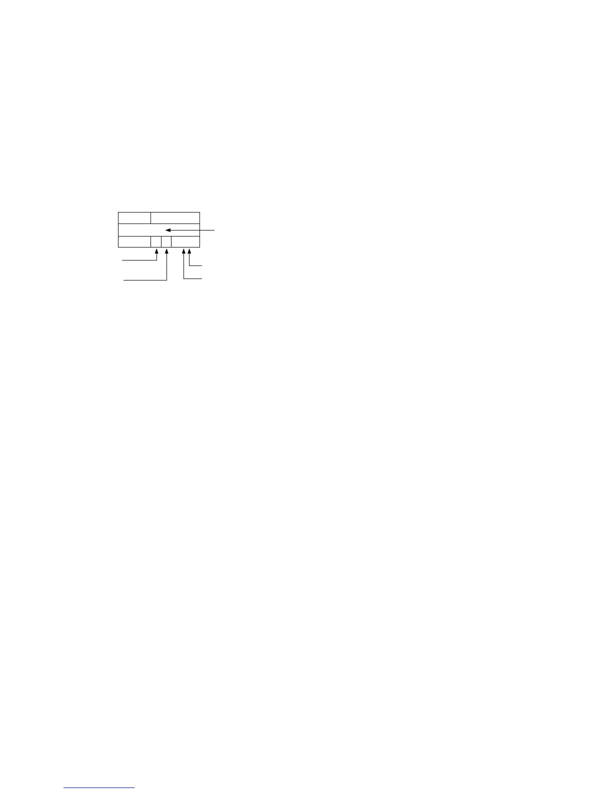
LOCATION
REF No.
IC101 B C 6 A
IC
Category : IC
Horizontal “A” zone
Vertical “6” zone
B : Foil side
(A : Component side)
C : Chip component
D : Discrete component)
 Loading...