(No.49837)1-45
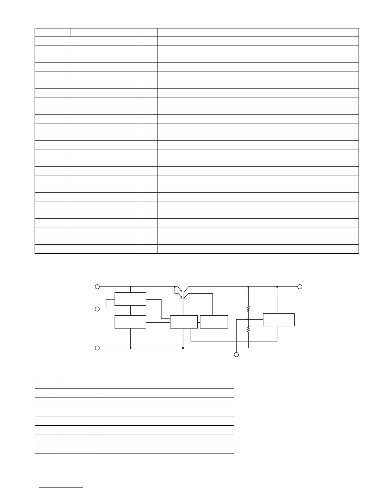
4.20 MM1565AF-X (IC108, IC261, IC551) : Regulator
• Block diagram
• Pin function
66 VIDEO ON/OFF O L: VIDEO OFF, H: VIDEO ON
67 BAND O Tuner receive band switching signal (H: FM, L: AM)
68 NC - Not connect
69 RXD0 I For flash ROM writing / UART(VCD status input)
70 TXD0 O For flash ROM writing / UART(VCD command output)
71 SD/ST I Station detection / FM stereo input
72 /MONO O FM monaural control output
73 IF/AGC O IF count request output
74 NC - Not connect
75 ANT.REMOTE O Antenna remote control output (H: tuner)
76 PARKING BRAKE I L: VIDEO OFF, H: VIDEO ON
77 NC - Not connect
78 SW1 I/O S1 input, Disc insert detection on power OFF
79 P.SAVE1 I Power save 1(ACC) detection, L: Power save
80 P.SAVE2 I Power save 2(BATTERY) detection, L: Power save
81 P.SAVE.SLAVE O Power save 1 control signal output to mecha micon
82 GND - Connect to ground
83 to 91 NC - Not connect
92 MUTE O Mute control signal output
93 TEL MUTING I Tel muting input
94 POWER CONT O Power supply IC control signal output
95 to 97 NC - Not connect
98 DETACH I Panel connector detection
99 VDDPORT - Connect to VDD
100 GNDPORT - Connect to ground
Pin No. Symbol I/O Function
Bias
Thermal
shutdown
Driver
Current
limiter
Reference
Vin
Cont
GND
Cn
Vo
Pin No. Symbol Function
1 Vout Output terminal
2 NC Non connect
3 GND Connect to ground
4 Cn Noise decrease terminal
5 Cout Control terminal
6 Sub Substrate (Connect to ground)
7 Vin Input terminal
 Loading...