MX-GA3V
1-22
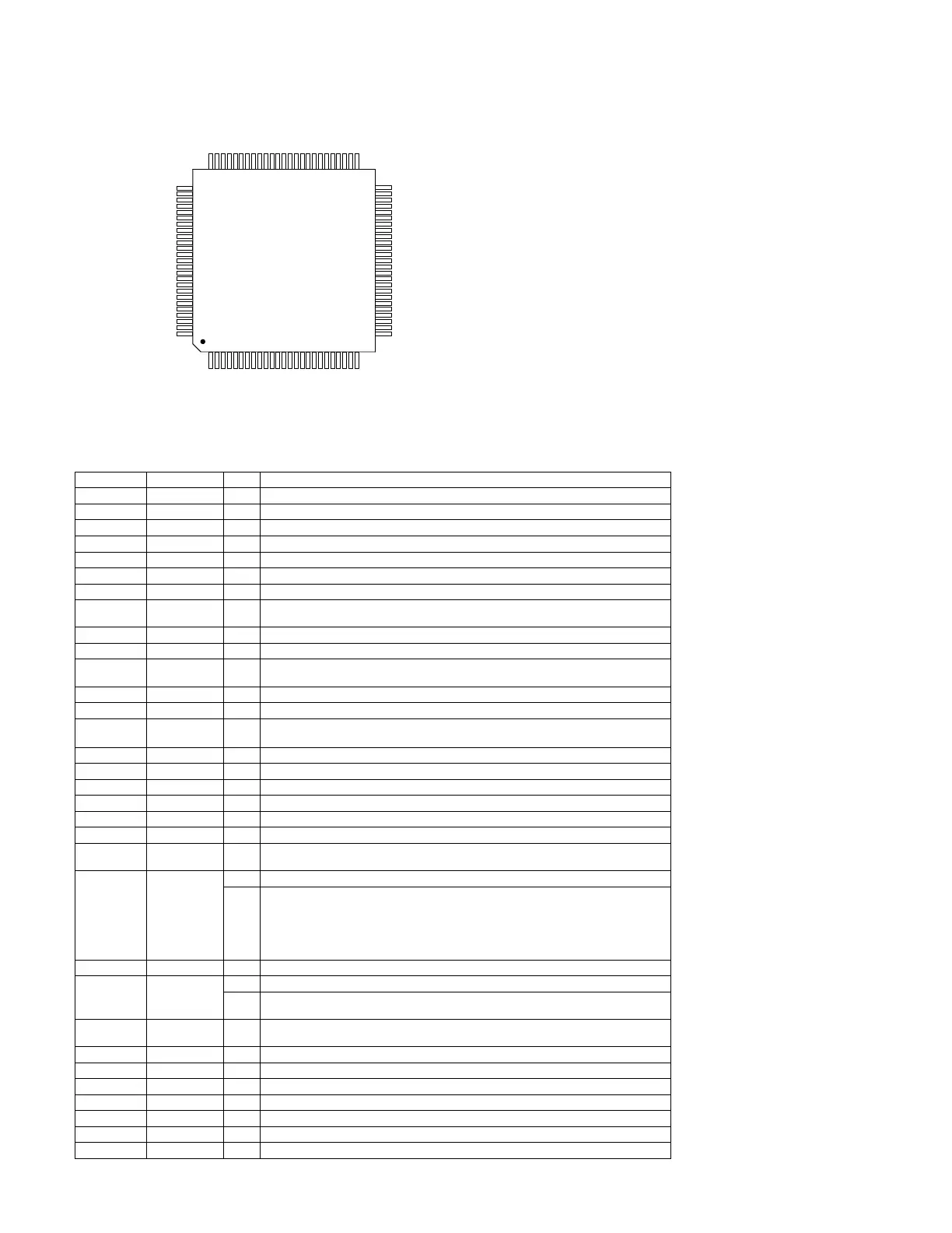
Figure 24 Visba Video CD Processor Chip Pinout Diagram
ESS
Visba ES3880
Video CD PC
100 TQFP
2
1
4
3
6
5
8
7
10
9
12
11
14
13
16
15
18
17
20
19
22
21
24
23
25
49
50
47
48
45
46
43
44
41
42
32
31
34
33
36
35
38
37
40
39
99
100
97
98
95
96
93
94
91
92
89
90
87
88
85
86
83
84
81
82
26
28
27
30
29
VSS
DBUS14
DBUS13
RESET#
DBUS15
AUX4
VSS
AUX2
AUX3
AUX0
AUX1
PCLK2X
PCLK
HSYNC
CPUCLK
YUV7
VSYNC
YUV5
YUV6
YUV3
YUV4
YUV1
YUV2
VDD
YUV0
75
73
74
71
72
69
70
67
68
65
66
63
64
61
62
59
60
57
58
55
56
53
54
51
52
79
80
77
78
76
LA7
LA5
LA6
LA3
LA4
LA1
LA2
LCS0#
LA0
LCS3#
LCS1#
LWR#
LOE#
LD6
LD7
LD4
LD5
LD2
LD3
LD0
LD1
AUX5
AUX7
VDD
AUX6
RAS#
VDD
DWE#
DA2
DA1
DA4
DA3
DA5
DA7
DA6
DBUS0
DA8
DBUS2
DBUS1
DBUS4
DBUS3
DBUS6
DBUS5
DBUS8
DBUS7
DBUS10
DBUS9
DBUS12
DBUS11
DA0
LA12
VPP
LA14
LA13
LA16
LA15
ACLK
LA17
ATCLK
AOUT/SEL_PLL0
DA9/DOE#
ATFS/SEL_PLL1
ARCLK
AIN
TDMCLK
ARFS
TDMFS
TDMDR
VSS
CAS#
LA11
VSS
LA9
LA10
LA8
Description of major ICs
VIDEO CD PROCESSOR CHIP PINOUT
VIDEO PC PROCESSOR CHIP PIN DESCRIPTION
Name Number I/O Definition
VDD 1, 31, 51 I Voltage supply for 3.3 V.
RAS# 2 O DRAM row address strobe (active low).
DWE# 3 O DRAM write enable (active low).
DA[8:0] 12:4 O DRAM multiplexed row and column address bus.
DBUS[15:0] 28:13 I/O DRAM data bus.
RESET# 29 I System reset (active low).
VSS 30, 50, 80, 100 I Ground.
YUV[7:0] 39:32 O Y is luminance, UV are chrominance data bus for screen video interface. YUV[7:0] for 8-
bit YUV mode.
VSYNC 40 I/O Vertical sync for screen video interface, programmable for rising or falling edge.
HSYNC 41 I/O Horizontal sync for screen video interface, programmable for rising or falling edge.
CPUCLK 42 I RISC and system clock input.
CPUCLK is used only if SEL_PLL[1:0] = 00.
PCLK2X 43 I/O Pixel clock; two times the actual pixel clock for screen video interface.
PCLK 44 I/O Pixel clock qualifier in for screen video interface.
AUX[7:0] 54, 52, 53,
49:45
I/O Auxiliary control pins (AUX0 and AUX1 are open collectors).
LD[7:0] 62:55 I/O RISC interface data bus.
LWR# 63 O RISC interface write enable (active low).
LOE# 64 O RISC interface output enable (active low).
LCS[3,1,0]# 65,66,67 O RISC interface chip select (active low).
LA[17:0] 87:82, 79:68 O RISC interface address bus.
VPP 81 I Digital supply voltage for 5 V.
ACLK 88 I/O Master clock for external audio DAC (8.192 MHz, 11.2896 MHz, 12.288 MHz, 16.9344
MHz, and 18.432 MHz).
AOUT/
SEL_PLL0
89 O Dual-purpose pin. AOUT is the audio interface serial data output
I Pins SEL_PLL[1:0] select phase-lock loop (PLL) clock frequency CPUCLK
for the Visba:
00 = bypass PLL.
01 = 54 MHz PLL.
10 = 67.5 MHz PLL.
11 = 81 MHz PLL.
ATCLK 90 I/O Audio transmit bit clock.
ATFS/
SEL_PLL1
91 O Dual-purpose pin. ATFS is the audio interface transmit frame sync.
I Pins SEL_PLL[1:0] select phase-lock loop (PLL) clock frequency CPUCLK for the Visba.
See the SEL_PLL0 pin above for the settings.
DA9/DOE# 92 O Dual purpose pin: DRAM output enable (active low)/DRAM multiplexed row and column
address bus.
AIN 93 I Audio interface serial data input.
ARCLK 94 I Audio receive bit clock.
ARFS 95 I Audio interface receive frame sync.
TDMCLK 96 I TDM interface serial clock.
TDMDR 97 I TDM interface serial data receive.
TDMFS 98 I TDM interface frame sync.
CAS# 99 O
DRAM column address strobe bank 0 (active low).
 Loading...