1-36
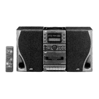
UX-A70MD
MCLK
CMODE
LRCK
SCLK
SDTO
SDTI
AINL
VCML
AINR
VCMR
VRAD
ARDV
VCOM
AOUTL
VA AGND VB VD DGND
AOUTR
PWAD PWDA
Clock
Divider
Serial I/O
Interface
Decimation
Filter
Decimation
Filter
8x
Interpolator
8x
Interpolator
Modulator
Modulator
Modulator
Modulator
Common Voltage
LPF
LPF
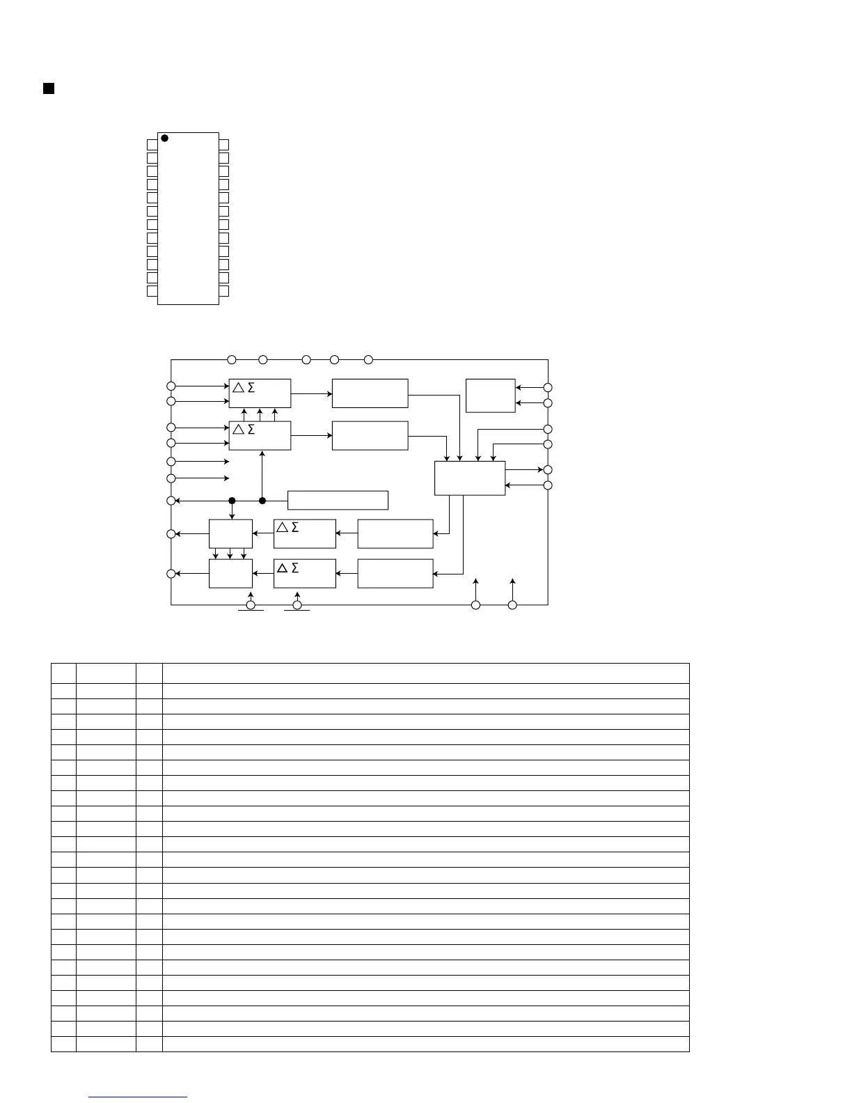
AK4519VF-X (IC480) : A / D D / A converter
1.Pin layout
2.Block diagram
3.Pin Function
1
2
3
4
5
6
7
8
9
10
11
12
24
23
22
21
20
19
18
17
16
15
14
13
1
2
3
4
5
6
7
8
9
10
11
12
13
14
15
16
17
18
19
20
21
22
23
24
I
I
I
O
O
I
I
I
I
I
I
O
-
-
I
I
I
I
O
O
O
-
-
-
VRDA
VRAD
AINR
VCMR
VCML
AINL
PWAD
PWDA
MCLK
LRCK
SCLK
SDTO
DGND
VD
SDTI
CMODE
DEM1
DEM0
AOUTL
AOUTR
VCOM
AGND
VB
VA
Voltage Reference Input Pin for DAC, VA
Voltage Reference Input Pin for ADC, VA
RCH Analog Input Pin
Rch Common Voltage Output Pin, 0.45xVA
Lch Common Voltage Output Pin, 0.45xVA
Lch Analog Input Pin
ADC Power-Down Mode Pin "L":Power Down
DAC Power-Down Mode Pin "L":Power Down
Master Clock Input Pin
Input/Output Channel Clock Pin
Audio Serial Data Clock Pin
Audio Serial Data Output Pin
Digital Ground Pin
Digital Power Supply Pin
Audio Serial Data Input Pin
Master Clock Select Pin
De-emphasis Frequency Select Pin
De-emphasis Frequensy Select Pin
Lch Analog Output Pin
Rch Analog Output Pin
Common Voltage Output Pin, 0.45xVA
Analog Ground Pin
Substrate Pin
Analog Power Supply Pin
Pin
NO.
Symbol I/O Function
Description of major ICs
 Loading...