4. Test mode of the unit
4-1 Setting of the test mode
While pressing the [REC/INPUT] key, plug the AC power
cord into the AC wall outlet.
4-2 Contents of the test mode
Choose the 3 mode by TIMER switch position below.
NONE means none mode.
(1) [ INSPECTION ] mode
•
ENGLISH display (2secs)
• " NIAGARA TEST " display
Dot : Niagara
Segment : All lighting
• Push a key, then cancel " NIAGARA TEST "
Display [ KEY 028 ] into the KEY-TEST mode.
Push a key, then display [ KEY
] .
(2) [ ERROR RATE ] mode
• Function of the key
• Function of the key
5. Microprocessor reset
The microprocessor can be initialized while pressing the
[EJECT] key, plug the AC power cord into the AC wall
outlet.
6. Mechanism test mode
Refer to 1050MD/DM-5090/MD-9090 service manual (B51-
5387-00), if you see this test mode.
TIMER SW Mode
(1) REC INSPECTION
(2) PLAY ERROR RATE
OFF NONE
Key Mode
REC/INPUT KEY-TEST
EDIT NIAGARA TEST
TITLE INPUT None all lighting
Key Function
PLAY CPLAY (MID)
REC CREC (MID)
STOP
STOP CPLAY, CREC
(2time push) ERROR RATE
Pin No. Port Name I/O Description
21 CS (SRAM) O SRAM control. chip select H : POWER DOWN
22 WR – SRAM control. write strobe signal output
23 RD – SRAM control. read strobe signal output
24-28 NC O no use
29-35 A14-8 – SRAM control. address bus
36-42 AD7-1 – SRAM control. address/data bus
43 AD0 – SRAM control. address/data bus L : POWER DOWN
44 ASTB – SRAM control. address strobe signal output
45 VSS – Microprocessor GND
46 TEST – Microprocessor TEST
47,48 NC O no use
49 MENA O Mechanism-microprocessor. enable
50 MRXD – Mechanism-microprocessor. data in line (UART)
51 MTXD O Mechanism-microprocessor. data out line (UART)
52-54 NC O no use
55 VDD – Microprocessor power supply (+)
56-61 NC I no use
62 CTR_JIS I Cyber titler. for JIS code H : JIS
63 TXT_JIS – CD TEXT. for JIS code H : JIS
64 AVDD – A/D power supply
65 AVref1 – A/D reference voltage input port (+5V)
66 AVSS – A/D GND
67,68 NC O no use
69 AVref2 – D/A reference voltage input port (+5V)
70 AVref3 – A/D reference voltage input port (GND)
71,72 NC I no use
73 DQSY – Text data read permit L : interrupt
74-76 NC I no use
77 CLOCK I IBM key board I/F clock line L : interrupt
78 SRDT I Text data read line
79 TRXD I Cyber titler. data in line (UART)
80 TTXD O Cyber titler. data out line (UART)
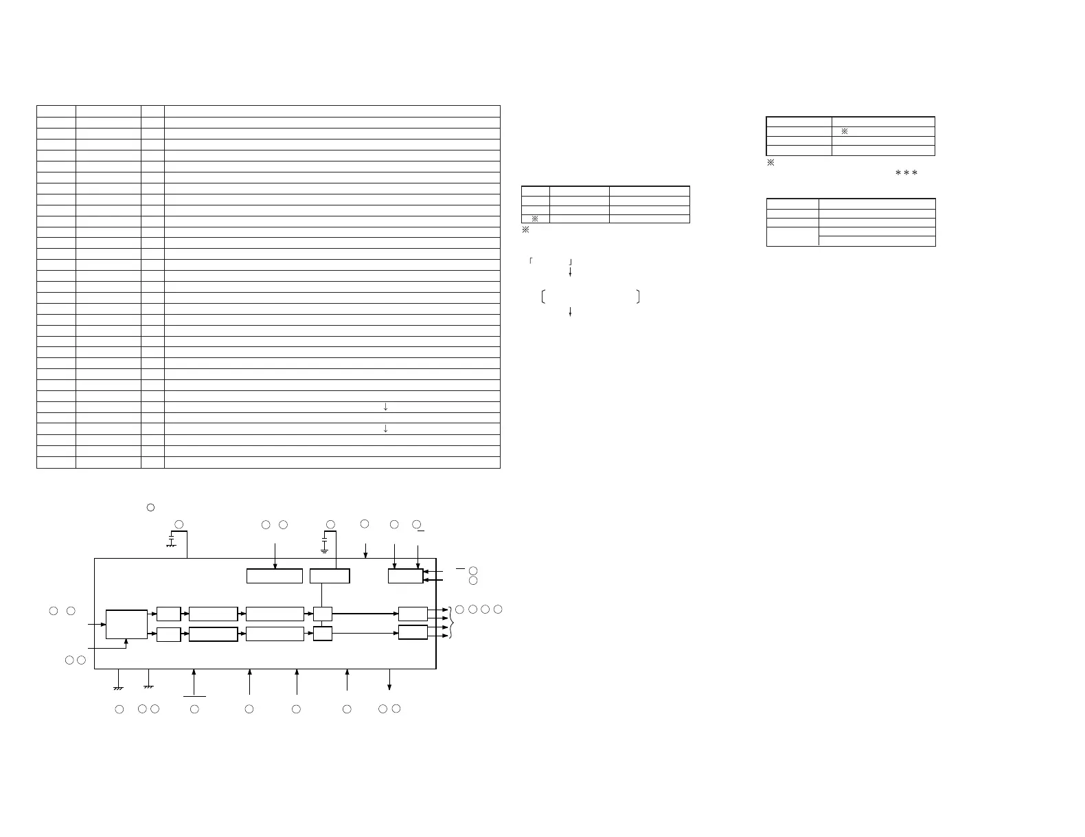
AD1855
SERIAL DATA
INTERFACE
16-/18-/20-/24-BIT
DIGITAL
DATA INPUT
25
~
27
3
19
~ 5
20 ,
1
9
8 ,
6
2
7
11 , 24
23
18
22
12 , , ,
10
28
14
13
16 17
15
21
SERIAL
MODE
DIGITAL
GND
ANALOG
GND
RD/RST
MUTE DE-EMPHASIS
ANALOG
SUPPLY
ZERO
FLAG
ANALOG
OUTPUTS
384/256
96/48Fs
CLOCK
DIGITAL
SUPPLY
CONTROL DATA
INPUT
CLOCK
IN
X2MCLK
ATTEN/
MUTE
8x
INTERPOLATOR
MULTIBIT SIGMA-
DELTA MODULATOR
OUTPUT
BUFFER
CLOCK
CIRCUIT
VOLTAGE
REFERENCE
SERIAL CONTROL
INTERFACE
OUTPUT
BUFFER
DAC
DAC
MULTIBIT SIGMA-
DELTA MODULATOR
8x
INTERPOLATOR
ATTEN/
MUTE
3. D/A converter : AD1855 (X25 : IC7)
Block diagram (No. of : pin No.)
 Loading...