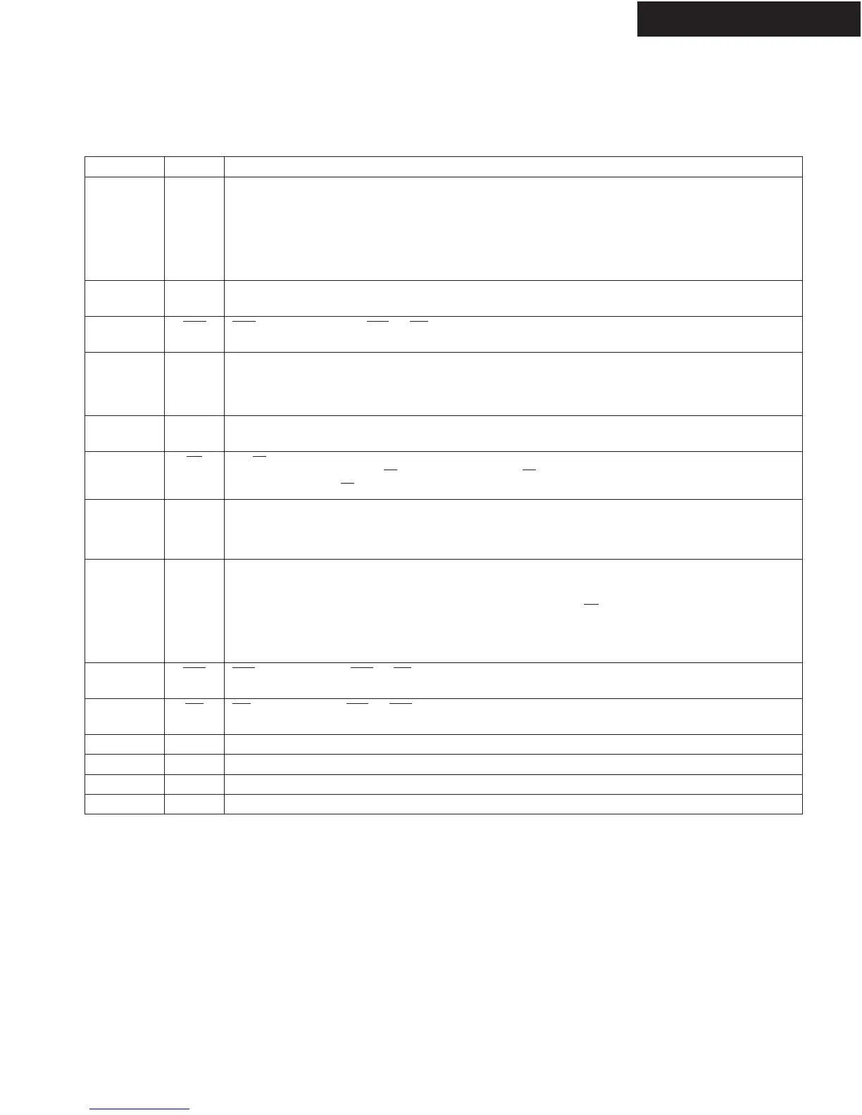
IC BLOCK DIAGRAM AND TERMINAL DESCRIPTIONS-16
Q7301: IC42S16100 (16-Mbit Synchronous Dynamic RAM)-2
TERMINAL DESCRIPTION
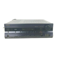
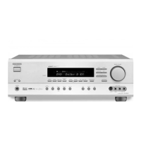
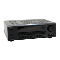
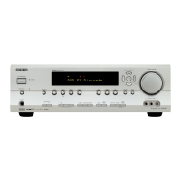
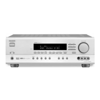
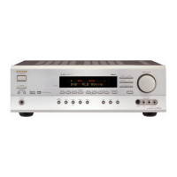
TX-SR502/E/8250/HT-R520
Pin No. Pin name Function (In Detail)
20 to 24
27 to 32
A0-A10 A0 to A10 are address inputs. A0-A10 are used as row address inputs during active command input
and A0-A7 as column address inputs during read or write command input. A10 is also used to
determine the precharge mode during other commands. If A10 is LOW during precharge command,
the bank selected by A11 is precharged, but if A10 is HIGH, both banks will be precharged.
When A10 is HIGH in read or write command cycle, the precharge starts automatically after
the burst access.
These signals become part of the OP CODE during mode register set command input.
19 A11 A11 is the bank selection signal. When A11 is LOW, bank 0 is selected and when high, bank 1 is
selected. This signal becomes part of the OP CODE during mode register set command input.
16 CAS CAS, in conjunction with the RAS and WE, forms the device command. See the "Command Truth
Table" item for details on device commands.
34 CKE The CKE input determines whether the CLK input is enabled within the device.
When is CKE HIGH, the next rising edge of the CLK signal will be valid, and when LOW, invalid.
When CKE is LOW, the device will be in either the power-down mode, the clock suspend mode,
or the self refresh mode. The CKE is an asynchronous input.
35 CLK CLK is the master clock input for this device. Except for CKE, all inputs to this device are acquired
in synchronization with the rising edge of this pin.
18 CS The CS input determines whether command input is enabled within the device.
Command input is enabled when CS is LOW, and disabled with CS is HIGH. The device remains in
the previous state when CS is HIGH.
2, 3, 5, 6, 8, 9,
11, 12, 39, 40,
42, 43, 45, 46,
48, 49
I/O0
to
I/O15
I/O0 to I/O15 are I/O pins. I/O through these pins can be controlled in byte units using the LDQM and
UDQM pins.
14, 36 LDQM,
UDQM
LDQM and UDQM control the lower and upper bytes of the I/O buffers. In read mode, LDQM and
UDQM control the output buffer. When LDQM or UDQM is LOW,
the corresponding buffer byte is enabled, and when HIGH, disabled. The outputs go to theHIGH
impedance state when LDQM/UDQM is HIGH. This function corresponds to OE in conventional
DRAMs. In write mode, LDQM and UDQM control the input buffer.
When LDQM or UDQM is LOW, the corresponding buffer byte is enabled, and data can be written to
the device. When LDQM or UDQM is HIGH, input data is masked and cannot be written to the device.
17 RAS RAS, in conjunction with CAS and WE, forms the device command. See the "Command Truth
Table" item for details on device commands.
15 WE WE, in conjunction with RAS and CAS, forms the device command. See the "Command Truth
Table" item for details on device commands.
7, 13, 38, 44 V
CCQVCCQ is the output buffer power supply.
1, 25 V
CC VCC is the device internal power supply.
4, 10, 41, 47 GNDQ GNDQ is the output buffer ground.
26, 50 GND GND is the device internal ground.
 Loading...