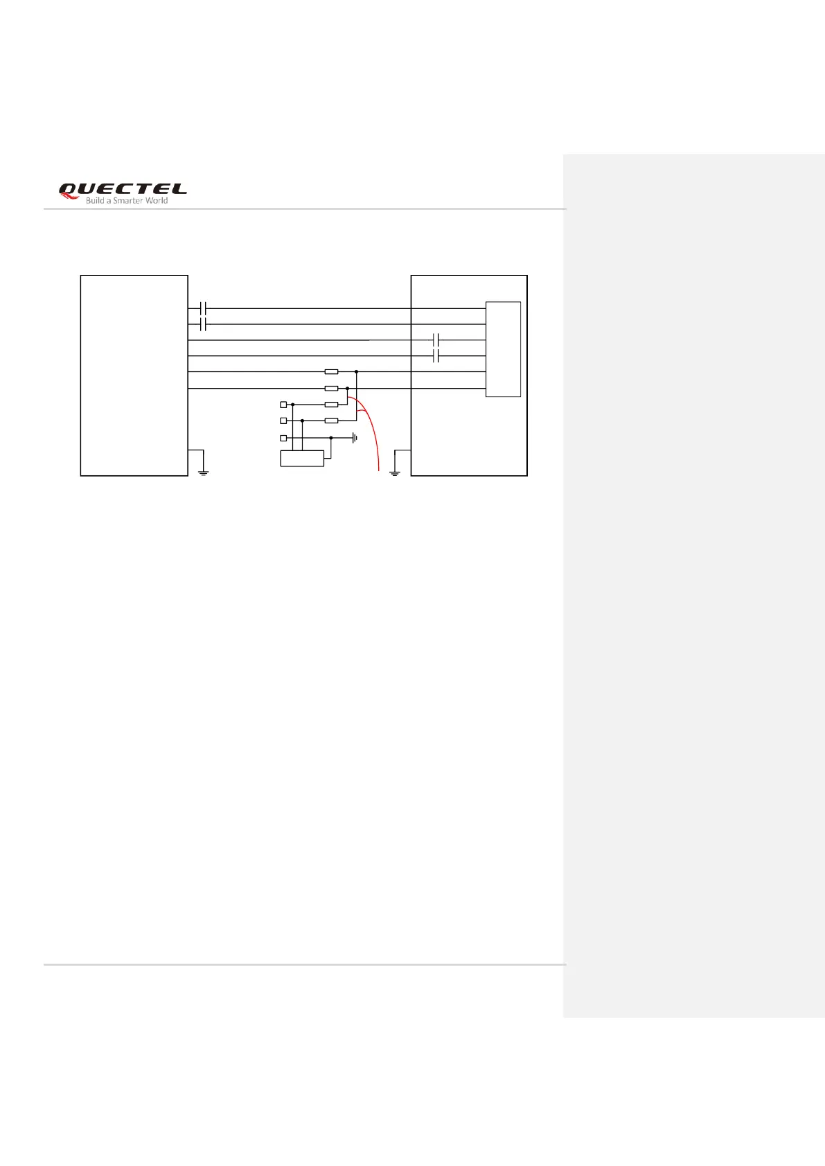
Figure 21: Reference Circuit of USB 3.0/2.0 Interface
AC coupling capacitors C5 and C6 must be placed close to the host and close to each other. C1 and C2
have been integrated inside the module, so do not place these two capacitors on customers’ schematic
and PCB. In order to ensure the signal integrity of USB 2.0 data traces, R1, R2, R3 and R4 components
must be placed close to the module, and the stubs must be minimized in PCB layout.
In order to ensure that the USB interface designs correspond with USB specifications, comply with the
following principles.
⚫ It is important to route the USB 2.0 & 3.0 signal traces as differential pairs with total grounding. The
impedance of USB differential trace is 90 Ω.
⚫ For USB 2.0 signal traces, the trace lengths must be less than 120 mm, and the differential data pair
matching is less than 2 mm (15 ps).
⚫ For USB 3.0 signal traces, the maximum length of TX and RX differential data pair is recommended
to be less than 100 mm, and the TX and RX differential data pair matching is less than 0.7 mm (5 ps).
⚫ Do not route signal traces under crystals, oscillators, magnetic devices or RF signal traces. It is
important to route the USB 2.0 & 3.0 differential traces in inner-layer with ground shielding on not
only upper and lower layers but also right and left sides.
⚫ If USB connector is used, keep the ESD protection components as close as possible to the USB
connector. Pay attention to the influence of junction capacitance of ESD protection components on
USB 2.0 & 3.0 data traces. Typically, the capacitance value should be less than 2.0 pF for USB 2.0,
and less than 0.4 pF for USB 3.0.
⚫ If possible, reserve four 0 Ω resistors (R1–R4) on USB_DP and USB_DM traces, as shown in the
above figure.

 Loading...