E2/E2 Lite Designing the User System
R20UT4582EJ0100 Rev.1.00 Page 11 of 30
Jul.16.19
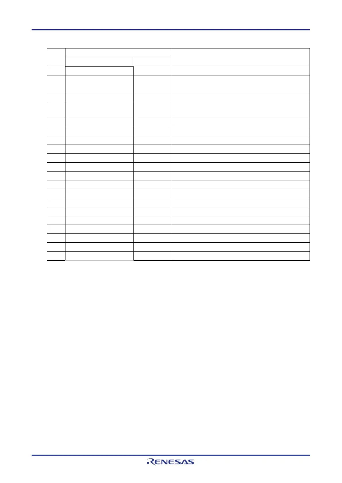
Table 2.3 Pin Assignments of the 20-Pin and 10-Pin Connectors for SWD Interface Connection
Pin
No.
R7F0E01 Group
Note
2 SWDIO/RxD9 I/O /
Input
Clock for debugging communications/
Communications data for flash programming
4 SWCLK/TxD9 Input/
Output
Clock for debugging communications/
Communications data for flash programming
6 NC –
8 NC –
10 RES# I/O User system reset
12 NC *4 –
14 NC *4 –
16 NC *4 –
18 NC *4 –
20 NC *4 –
Notes: 1.
These are the names of the MCU pins at the time the E2/E2 Lite is connected (i.e. during
debugging).
2. Input to or output from the user system.
3.
Securely connect pins 3, 5, 9, 15, 17, and 19 of the connector to GND on the user system.
These pins are used for electrical grounding as well as for monitoring of connection with the
user system by the E2/E2 Lite.
4.
If a 10-pin (1.27-mm pin pitch) connector is mounted on the user system, pins 11 to 20 are
not used.
 Loading...


