RC22312A/RC32312A Evaluation Board Manual
R31UH0022EU0100 Rev.1.00
Mar 28, 2023
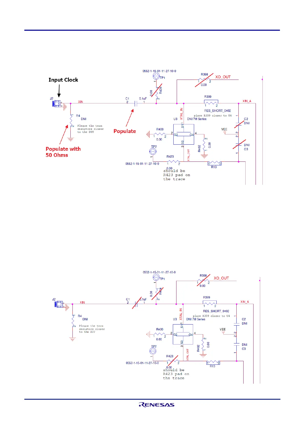
2. Depopulate C2, C3, R398, and R424 to ensure that excess trace is not used.
3. Populate R4 with 50Ω for input termination (ensure signal is >~1.3V amplitude).
4. Place input clock signal at J2 and ensure that the signal is within specification for the XIN pin.
Figure 8. XIN Pin Overdrive Schematic
1.2.3. On-board Crystal Mount
The crystal mounting position can only be used if there is no other signal present on the XIN path (see Figure 9).
In order to setup the evaluation board for crystal input:
1. Depopulate C1, R398, R423, and R424 to ensure there is no excess trace in the XIN pin.
2. Populate C2 and C3 to externally tune the input crystal frequency.
Note: The EVB stray capacitance has been measured to be ~8.24pF.
3. Mount crystal to U3. Remove R400 or R402 if the crystal only has 3 pads.
Figure 9. Crystal Mount Schematic
 Loading...