R-210D
15
DESCRIPTION OF LSI
LSI(IXA023DR)
The I/O signal of the LSI(IXA023DR) are detailed in the following table.
Pin No. Signal I/O Description
1 D3 OUT Segment data signal.
Signal is input to the cathodes of the light-emitting diodes (LD8, LD16 and LD24).
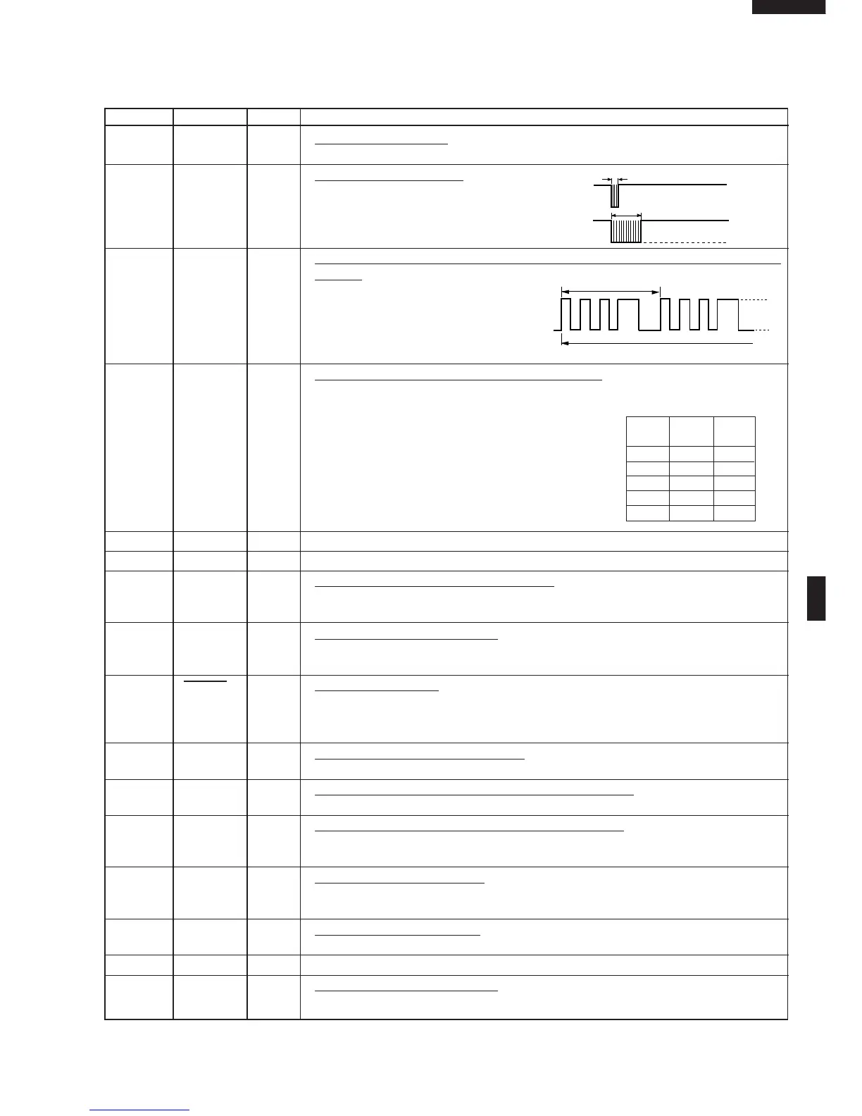
2 D4 OUT Signal to sound buzzer.
A: Tact switch touch sound.
B: Completion sound.
3 D5 OUT Oven lamp, turntable motor and fan motor driving signal(Square Waveform
: 50Hz).
To turn on and off shut-off relay
(RY1). The square waveform volt-
age is delivered to the relay (RY1)
driving circuit and relay(RY2) con-
trol circuit.
4 D6 OUT Magnetron high-voltage circuit driving signal.
To turn on and off the cook relay (RY2). In
100% power operation, the signals hold
"L" level during microwave cooking and
"H" level while not cooking. In other cook-
ing modes (70%, 50%, 30%, 10%) the
signal turns to "H" level and "L" level in
repetition according to the power level.
5 D7 IN/OUT Terminal not used.
6 P20 IN Connected to 0V.
7 P21 IN Signal coming from touch tact switch.
When tact switch SW2 is touched, a signal will be input into P21. When tact switch
is not touched, the signal is held at "H" level.
8 P22 IN Signal coming from encoder.
When the encoder is turned, the contacts of encoder make pulse signals. And
pulse signals are input into P22.
9
RESET
IN Auto clear terminal.
Signal is input to reset the LSI to the initial state when power is applied. Temporarily
set to "L" level the moment power is applied, at this time the LSI is reset. Thereafter
set at "H" level.
10 CNVSS IN Reference voltage input terminal.
A reference voltage is applied to the A/D converter in the LSI. Connected to VC.
11 XOUT OUT Internal clock oscillation frequency control output.
Output to control oscillation input of XOUT.
12 XIN IN Internal clock oscillation frequency input setting.
The internal clock frequency is set by inserting the ceramic filter oscillation circuit
with respect to XIN terminal.
13 VSS IN Power source voltage: -5V.
The power source voltage to drive the LSI is input to VSS terminal. Connected to
VC.
14 VDD IN Power source voltage: 0V.
The power source voltage to drive the LSI is input to VDD terminal.
15 N.F IN Connected to VSS terminal.
16 INT0 IN Signal coming from encoder.
Signal similar to INT0. Pulse signals are input into INT0.
A
B
H: GND
L: -5V
0.12 sec
2.4 sec
20 msec
During cooking
H
L
ON/OFF time ratio in Mi-
cro cooking
(a. 27second time base)
MICRO ON OFF
COOK
100% 27sec. 0sec.
70% 21sec. 6sec.
50% 15sec. 12sec.
30% 9sec. 18sec.
10% 5sec. 22sec.
 Loading...