SLT-A33/A33L/A33Y/A55/A55V/A55L/A55VL/A55VY_L3
6-1
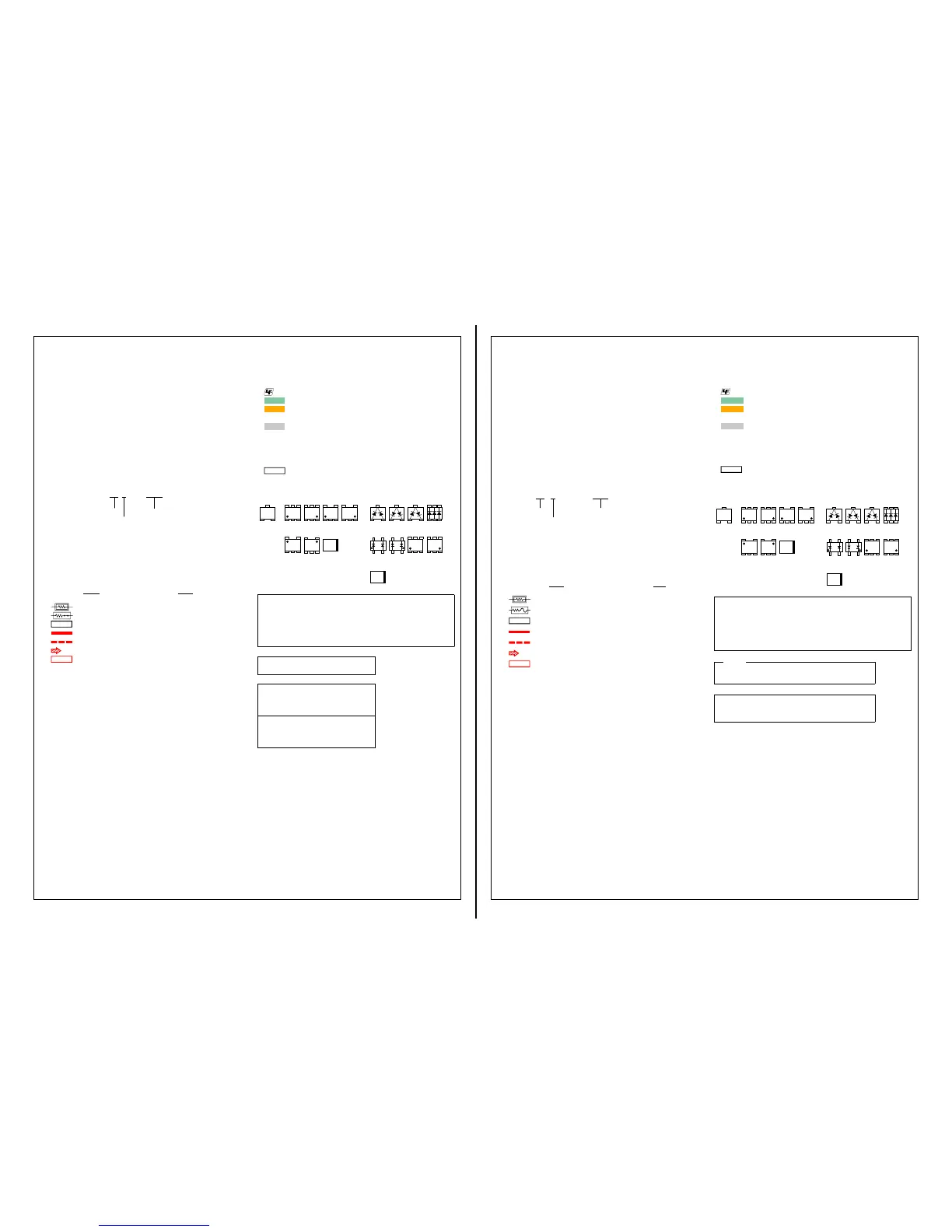
回路図ノート
・ ケミコン,タンタルを除くコンデンサで,耐圧50V以下の
ものはその耐圧を省略。単位はすべてμF(pはpF)。
・ チップ抵抗で指示のないものは,1/10W以下。
kΩ=1000Ω,MΩ=1000kΩ
・ チップ部品交換時の注意
取り外した部品は再使用せず,未使用の部品をご使用く
ださい。
タンタルコンデンサのマイナス側は熱に弱いため注意し
てください。
・ チップ部品には下記のように表示したものがあります。
例 C541 L452
22U 10UH
TA A 2520
種類 外形寸法(mm)
ケースサイズ
・ 抵抗,コンデンサ,ICなど定数にXXがあるものは,使用
していない事を示しています。このため,使用していな
い回路が記載されている事があります。
・ ★印のある部品は,機種などにより異なりますので機能
別マウント一覧表を参照してください。
・ 可変抵抗と半固定抵抗で,B特性の表示を省略。
・ 信号名表記について,下記のような場合があります。
XEDIT → EDIT PB/XREC → PB/REC
・
は不燃性抵抗。
・ はヒューズ抵抗。
・ はパネル表示名称。
・ はB+ライン。
・ はB-ライン。
・ はBライン(+,-)の入出力方向を示す。
・ は調整名称。
6. SCHEMATIC DIAGRAMS AND PRINTED WIRING BOARDS
THIS NOTE IS COMMON FOR SCHEMATIC DIAGRAMS AND PRINTED WIRING BOARDS
(In addition to this, the necessary note is printed in each block)
– ENGLISH –
2 1
3
2 1
3
2 1
3
345
21
123
654
EB
C
31
5
2
46
123
654
31
5
2
46
123
54
4 3
1 2
31 2
45
53 4
12
14
23
46
2
5
31
12
4
3
14
23
For Schematic Diagrams
• All capacitors are in μF unless otherwise noted. pF : μ
μF. 50 V or less are not indicated except for electrolytics
and tantalums.
• Chip resistors are 1/10 W unless otherwise noted.
kΩ=1000 Ω, MΩ=1000 kΩ.
• Caution when replacing chip parts.
New parts must be attached after removal of chip.
Be careful not to heat the minus side of tantalum
capacitor, Because it is damaged by the heat.
• Some chip part will be indicated as follows.
Example C541 L452
22U 10UH
TA A 2520
Kinds of capacitor External dimensions (mm)
Case size
• Constants of resistors, capacitors, ICs and etc with XX
indicate that they are not used.
In such cases, the unused circuits may be indicated.
• Parts with ★ differ according to the model/destination.
Refer to the mount table for each function.
• All variable and adjustable resistors have characteristic
curve B, unless otherwise noted.
• Signal name
XEDIT → EDIT PB/XREC → PB/REC
•
: non flammable resistor
•
: fusible resistor
•
: panel designation
•
: B+ Line
•
: B– Line
•
: IN/OUT direction of (+, –) B LINE.
•
: adjustment for repair.
The components identified by mark 0
or dotted line with mark 0 are critical
for safety.
Replace only with part number specified.
Les composants iden tif iés par une
marque 0 sont critiques pour la sécurité.
Ne les remplacer que par une pièce
portant le numéro spécifié.
When indicating parts by reference
number, please include the board name.
For Printed Wiring Boards
• : Uses unleaded solder.
•
: Circuit board
: Flexible board
Pattern from the side which enables seeing.
: pattern of the rear side
(The other layers’ patterns are not indicated)
• Through hole is omitted.
• There are a few cases that the part printed on diagram
isn’t mounted in this model.
•
: panel designation
• Chip parts.
Transistor Diode
回路図,プリント図共通ノート
(他に必要なノートは各セクションに記載しています)
プリント図ノート
・ :無鉛半田を使用しています。
・ :基板
:フレキシブル配線板
見ている面側のパターン。
:裏側のパターン
(他のパターンについては表示されていません)
・ スルーホールは省略。
・ プリント図には,本機で使用していない部品が記載さ
れている場合があります。
・ はパネル表示名称。
• Chipparts.
Transistor Diode
2 1
3
2 1
3
2 1
3
345
21
123
654
EB
C
31
5
2
46
123
654
31
5
2
46
123
54
4 3
1 2
31 2
45
53 4
12
14
23
46
2
5
31
12
4
3
14
23
0
印の部品,または
0
印付の点線で囲まれた部品は,
安全性を維持するために,重要な部品です。
従って交換時は,必ず指定の部品を使用してください。
図面番号で部品を指定するときは基板名又はブロック
を併せて指定してください。
お願い
– JAPANESE –
Precautions for Replacement of Imager
• If the imager has been replaced, carry out all the adjustments
for the camera section.
• As the imager may be damaged by static electricity
from its structure, handle it carefully like for the MOS IC.
In addition, ensure that the receiver is not covered with dusts nor
exposed to strong light.
イメージャ交換時の注意
・ イメージャを交換した場合は,カメラ部の全調整を行って
ください。
・ イメージャは構造上,静電気により破壊される恐れがあるため,
MOSICと同様に注意して取り扱ってください。
また,受光部にはゴミの付着,および強い光がはいることのない
ように注意してください。
 Loading...