2
SS-CT52/TS53/TS54/TS55/TS56W/WS53
SECTION 1
DIAGRAMS
For Schematic Diagrams.
Note:
• All capacitors are in µF unless otherwise noted. (p: pF)
50 WV or less are not indicated except for electrolytics and
tantalums.
• All resistors are in Ω and
1
/
4
W or less unless otherwise
specified.
• C : panel designation.
THIS NOTE IS COMMON FOR PRINTED WIRING BOARDS AND SCHEMATIC DIAGRAMS.
(In addition to this, the necessary note is printed in each block.)
• A : B+ Line.
•Voltages are dc with respect to ground under no-signal
(detuned) conditions.
•Voltages are dc with respect to ground in service mode.
no mark : DVD STOP
•Voltages are taken with VOM (Input impedance 10 MΩ).
• Circled numbers refer to waveforms.
• Signal path.
F : AUDIO
For Printed Wiring Boards.
Note:
• X : parts extracted from the component side.
• a : Through hole.
•
: Pattern from the side which enables seeing.
(The other layers' patterns are not indicated.)
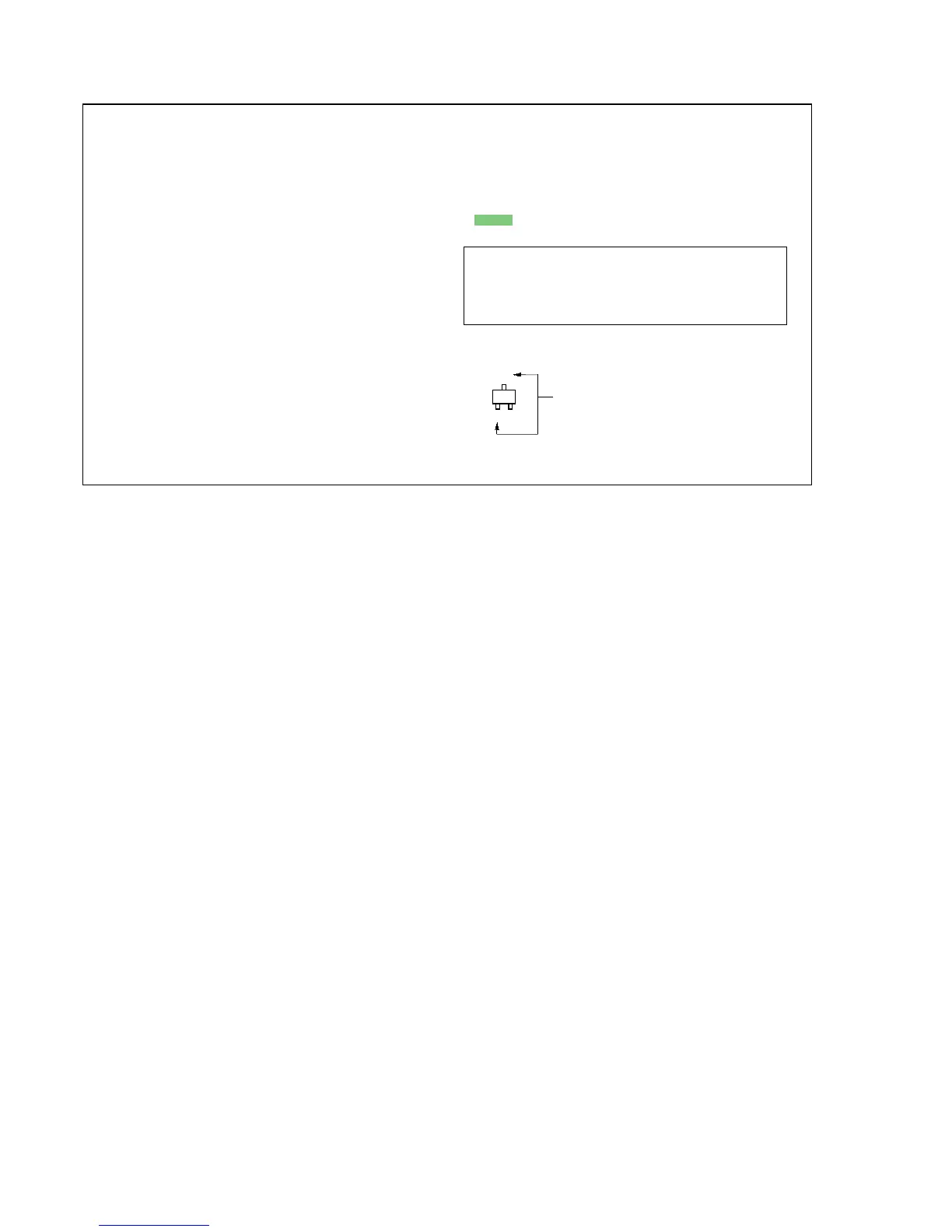
• Indication of transistor.
Caution:
Pattern face side: Parts on the pattern face side seen from
(SIDE B) the pattern face are indicated.
Parts face side: Parts on the parts face side seen from
(SIDE A) the parts face are indicated.
C
B
These are omitted.
E
Q
 Loading...