1-2. CIRCUIT DESCRIPTION
PROTECTION CIRCUIT
Two kinds of protection circuit are employed in
this power amplifier. One is a power-transistor
protection circuit and the other is a speaker pro-
tection circuit.
1. Power-transistor Protection Circuit
To protect overloaded power transistors from
destruction, a protection circuit is employed. The
fusible resistors are inserted in each of Q704,
4705
(L-CH)
and 4754, 4755 (R-CH) collector
and emitter circuits. When the excessive current
flows into the power transistors, these fusible
resistors break faster than the transistors and thus
protects the transistors from destruction.
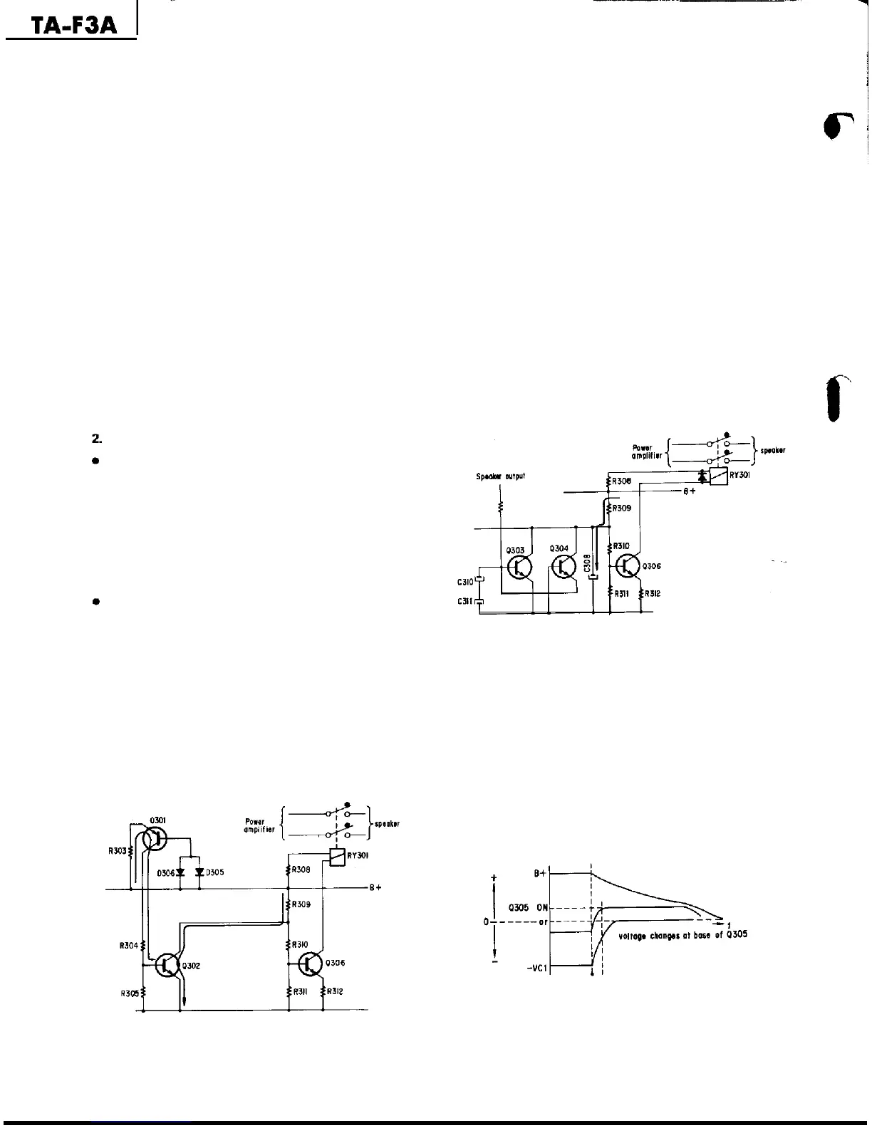
Speaker Protection Circuit
(See
Fig. l-l and Fig.
1-2)
When the excessive current flows into the power
transistors,
B+
voltage decreases. Therefore, 4301
turns on, biasing the base of
Q302,
and Q302
conducts. This removes the bias voltage at the
base of
Q306
and Q306 turns off. The relay is
not activated by off state of Q306. According-
ly, the speaker is cut off from the amplifier
circuit.
When the positive dc component presents at the
speaker output terminal,
C310
is charged up as
shown in Fig. l-2. Q303 turns on, Q306 turns off
and the relay RY301 is not activated (4304 re-
mains in off condition). Also, when the negative
dc component presents, C3 11 is charged up. This
turns 9304 on,
Q306
off and RY301 is not
activated (9303 remains in off condition).
3.
.
Muting Circuit
(See
Fig. 1-3 and Fig.
1-4)
This muting circuit prevents the loud “pop” (due
to initial current flow) or click noises produced
just after turning the POWER switch to on or off.
These transients might
damage a delicate high-
fidelity speaker system.
When POWER
Switch turned on:
C308
commerces
to charge through R309. At the
same time, the base voltage of
Q306
gradually
rises in accordance with charging voltage of
C308.
It takes about 3 seconds until
Q306
is turned on.
Accordingly, the speaker output terminal is cut off
by the relay
RY301
for about 3 seconds after the
POWER switch is turned on. This protects
the
speaker from the destruction caused by the “pop”
noises.
.
When
POWER
Switch turned off:
Fig.
1-2.
The reverse voltage (about
-
1.7 V) that turns off
Q306 immediately reduces, and the positive poten-
tial is applied to the base of
Q305.
Q305 turns on
and Q306 turns off, cutting off the operation of
RY301. Therefore, no pop noise presents on the
speaker output.
POWER
Switch
:ON
Fig. l-1.
-4-
Fig. 1-3.
 Loading...