Hardware layout and configuration UM1724
26/68 UM1724 Rev 14
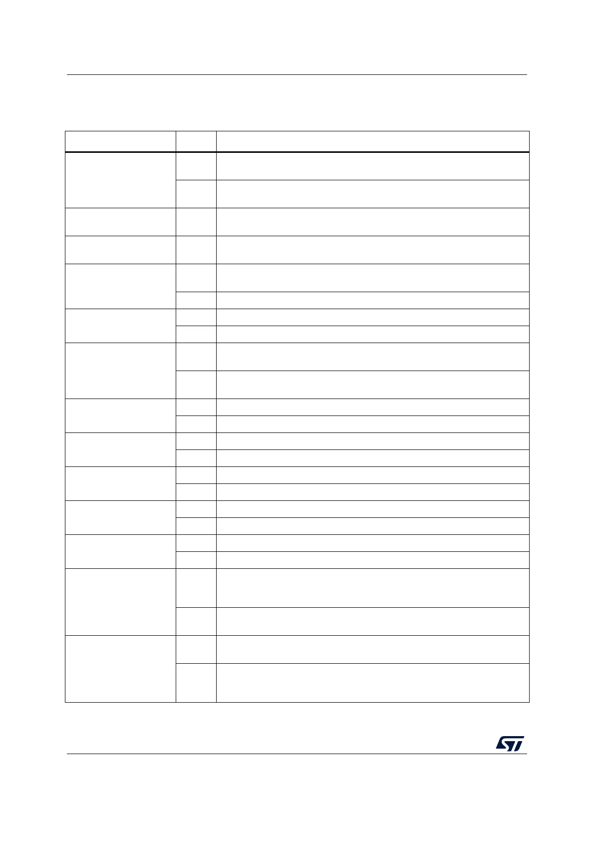
6.9 Solder bridges
Table 10. Solder bridges
Bridge State
(1)
Description
SB54, SB55 (X3 crystal)
(2)
OFF
X3, C33, C34, R35, and R37 provide a clock as shown in electrical
schematics PF0/PD0/PH0, PF1/PD1/PH1 are disconnected from CN7.
ON
PF0/PD0/PH0 and PF1/PD1/PH1 are connected to CN7. (R35, R37, and
SB50 must not be fitted).
SB3, SB5, SB7,SB9
(DEFAULT)
ON Reserved, do not modify.
SB4,SB6, SB8,SB10
(RESERVED)
OFF Reserved, do not modify.
SB48, SB49
(X2 crystal)
(3)
OFF
X2, C31, C32, R34, and R36 deliver a 32 kHz clock. PC14, PC15 are not
connected to CN7.
ON PC14 and PC15 are only connected to CN7. Remove only R34, R36.
SB17
(B1-USER)
ON B1 push button is connected to PC13.
OFF B1 push button is not connected to PC13.
SB12 (NRST)
ON
The NRST signal of the CN4 connector is connected to the NRST pin of the
STM32.
OFF
The NRST signal of the CN4 connector is not connected to the NRST pin of
the STM32.
SB15 (SWO)
ON The SWO signal of the CN4 connector is connected to PB3.
OFF The SWO signal is not connected.
SB11 (STM_RST)
OFF No incidence on STM32F103CBT6 (ST-LINK MCU) NRST signal.
ON STM32F103CBT6 (ST-LINK MCU) NRST signal is connected to GND.
SB1 (USB-5V)
OFF USB power management is functional.
ON USB power management is disabled.
SB2 (3.3 V)
ON Output of voltage regulator LD39050PU33R is connected to 3.3V.
OFF Output of voltage regulator LD39050PU33R is not connected.
SB21 (LD2-LED)
ON Green user LED LD2 is connected to D13 of
ARDUINO
®
signal.
OFF Green user LED LD2 is not connected.
SB56,SB51 (A4 and A5)
ON
PC1 and PC0 (ADC in) are connected to A4 and A5 (pin 5 and pin 6) on
ARDUINO
®
connector CN8 and ST morpho connector CN7. Thus SB46 and
SB52 must be OFF.
OFF
PC1 and PC0 (ADC in) are disconnected to A4 and A5 (pin 5 and pin 6) on
ARDUINO
®
connector CN8 and ST morpho connector CN7.
SB46,SB52
(I2C on A4 and A5)
OFF
PB9 and PB8 (I2C) are disconnected to A4 and A5 (pin 5 and pin 6) on
ARDUINO
®
connector CN8 and ST morpho connector CN7.
ON
PB9 and PB8 (I2C) are connected to A4 and A5 (pin 5 and pin 6) on
ARDUINO
®
connector CN8 and ST morpho connector CN7 as I2C signals.
Thus SB56 and SB51 must be OFF.
 Loading...


