DocID028406 Rev 1 21/31
UM1956 Hardware layout and configuration
30
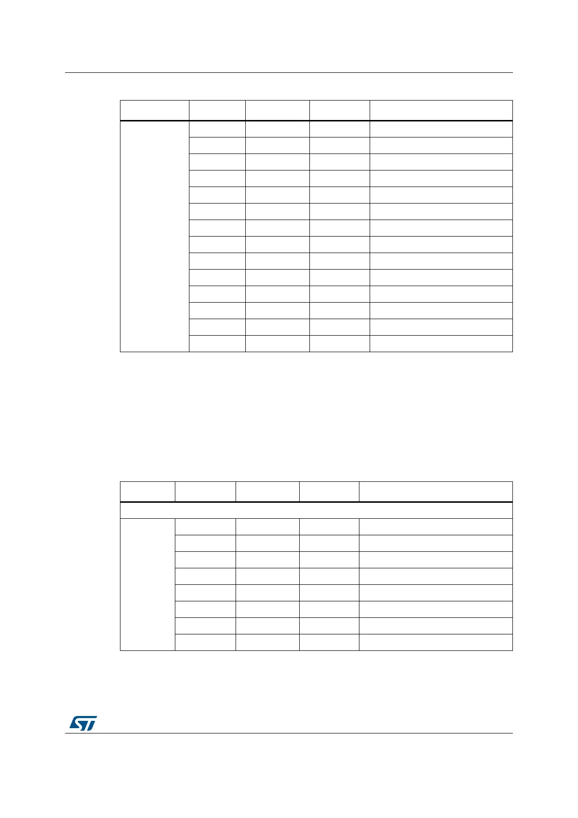
CN4
2 GND - Ground
3 RESET NRST RESET
4 +5V - 5V input/output
5 A7 PA2 ADC_IN2
6 A6 PA7 ADC_IN7
7A5
(5)
PA6 ADC_IN6 || I2C1_SCL
8A4
(5)
PA5 ADC_IN5 || I2C1_SDA
9 A3 PA4 ADC_IN4
10 A2 PA3 ADC_IN3
11 A1 PA1 ADC_IN1
12 A0 PA0 ADC_IN0
13 AREF - AVDD
14 +3V3 - 3.3V input/output
15 D13 PB3 SPI1_SCK
1. Only one USART is available and it is shared between Arduino Nano and VCP. The selection is done by
remapping (no need to change the hardware configuration).
2. D5 PWM on inverted channel Timer 16.
3. D7/D8 shared with OSC_IN/OSC_OUT.
4. SPI_CS is made by GPIO.
5. Limitations on A4 and A5, D4 and D5 related to I2C configuration are explained in Section 6.8: Solder
bridges according to SB16/SB18 setting.
Table 9. Arduino Nano connectors on NUCLEO-F042K6
Connector Pin number Pin name STM32 pin Function
Left connector
CN3
1D1PA9 USART1_TX
2 D0 PA10 USART1_RX
3 RESET NRST RESET
4 GND - Ground
5D2PA12 -
6 D3 PB0 TIM3_CH3
7D4
(1)
PB7 -
8D5
(1)
PB6 TIM16_CH1N
(2)
Table 8. Arduino Nano connectors on NUCLEO-F031K6 (continued)
Connector Pin number Pin name STM32 pin Function
 Loading...