Do you have a question about the Xilinx MicroBlaze and is the answer not in the manual?
| Architecture | 32-bit RISC |
|---|---|
| Cache | Configurable Instruction and Data Cache |
| Category | Soft Processor Core |
| Data Width | 32-bit |
| Memory Management Unit (MMU) | Optional |
| Floating Point Unit (FPU) | Optional |
| Interrupt Controller | Configurable |
| Memory Management | Optional MMU |
| Configurability | Highly Configurable |
| Pipeline Stages | 3-stage |
| FPGA Integration | Xilinx FPGAs |
| Bus Interface | PLB |
| Debug Interface | JTAG |
| Typical Clock Speed | Varies depending on FPGA and configuration (e.g., 100-400+ MHz) |
| Implementation | Soft core (synthesized logic) |
| Maximum Performance | Varies with FPGA and configuration |
| Debug Support | Integrated Debug Module |
Details the block diagram of the MicroBlaze Microcontroller used in this reference design, including components like RAM, UART, and GPIO.
Details the microprocessor, including speed, cache options, registers, and execution.
Covers dual port 16 KB blockRAM memory structure and the RS232 UART Controller.
Describes GPIO ports for LEDs and switches, and the JTAG_UART core for debugging with XMD and GDB.
Lists required software (Windows, EDK, ISE) and hardware (Evaluation Board, cables) for this reference design.
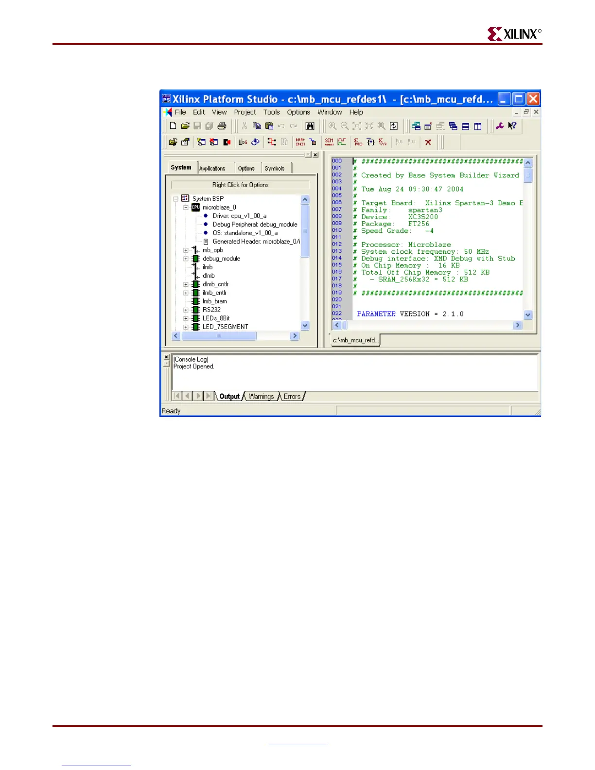
Procedure to select software application options in XPS for loading after the FPGA is configured and processor is running.