Virtex-5 FPGA ML561 User Guide www.xilinx.com 21
UG199 (v1.2.1) June 15, 2009
Memory Details
R
Memory Details
DDR400 and DDR2 Component Memories
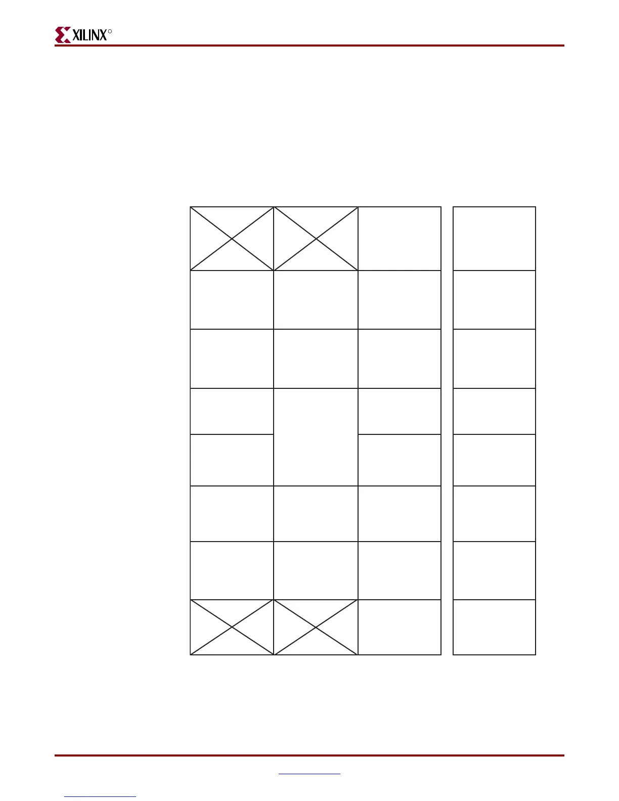
The FPGA #1 device on the Virtex-5 FPGA ML561 Development Board is connected to
DDR and DDR2 component memories, as shown in Figure 3-3.
Figure 3-3 summarizes the distribution of DDR and DDR2 discrete component interface
signals among the different banks of the FPGA #1 device.
Figure 3-3: FPGA #1 Banks for DDR400 and DDR2 Component (Top View)
BANK 21 (40)
BANK 13 (40)
DDR Components
DQ 0, 1, 2
BANK 114
BANK 112
BANK 11 (40)
DDR Components
DQ 3 & Controls
BANK 12 (40)
USB Controls
BANK 17 (40) BANK 18 (40) BANK 118
BANK 22 (40) BANK 122
BANK 126
(Configuration)
BANK 0
BANK 4 (20)
Global Clock Inputs
BANK 25 (40) BANK 6 (20)
GTP I/O
BANK 2 (20)
Voltage Control
BANK 15 (40)
DDR2 Component
DQ 0, 1
BANK 116
BANK 19 (40)
DDR2 Component
DQ 2, 3
BANK 120BANK 20 (40)
RS232
Inter-FPGA MII Links
BANK 1 (20)
DDR2 Component
Address
BANK 23 (40) BANK 124BANK 5 (20)
BANK 3 (20)
DDR2 Component
Controls
UG199_c3_03_050106
 Loading...


