3.15 Audio configuration
The FPGA design implements a simple serial interface that is based on I
2
C.
The following table describes the registers for the audio I
2
C control interface:
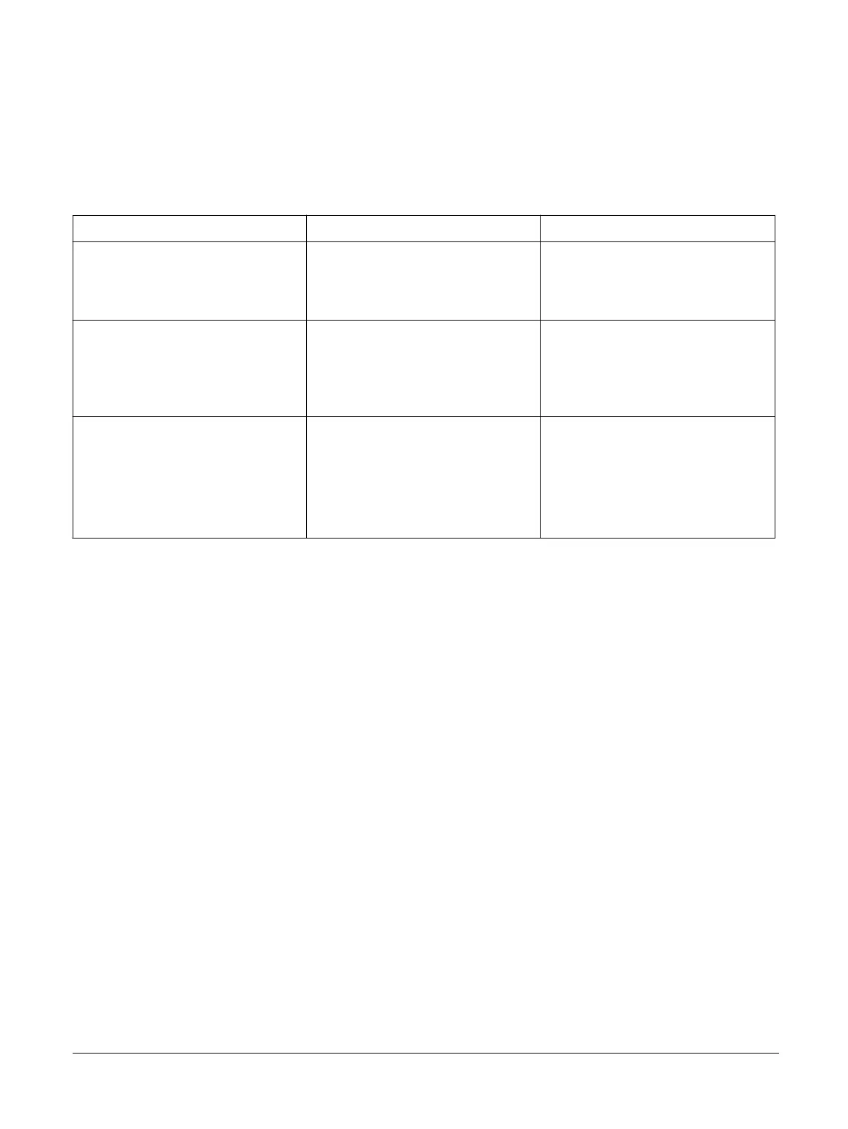
Table 3-3 I
2
C control interface registers
Address Name Description
0x40023000
CONTROL Reads from this register return:
1 Serial Data (SDA) input
0 Serial Clock (SCL) output
0x40023000
SET[1:0] Bits written as 0b1 set the appropriate
output bit:
1 SDOUTEN_n
0 SCL
0x40023004
CLEAR[1:0] Bits written as 0b1 clear the appropriate
output bit:
1 SDOUTEN_n
0 SCL
Reads from this register return 0b00.
The serial data is driven LOW when SDOUTEN_n is driven high, otherwise it is configured as an input
pin.
The audio I
2
C control interface drives the Cirrus Logic CS42L52 codec chip on the baseboard.
3 FPGA platform overview
3.15 Audio configuration
ARM 100896_0000_00_en Copyright © 2017 ARM Limited or its affiliates. All rights reserved. 3-40
Non-Confidential