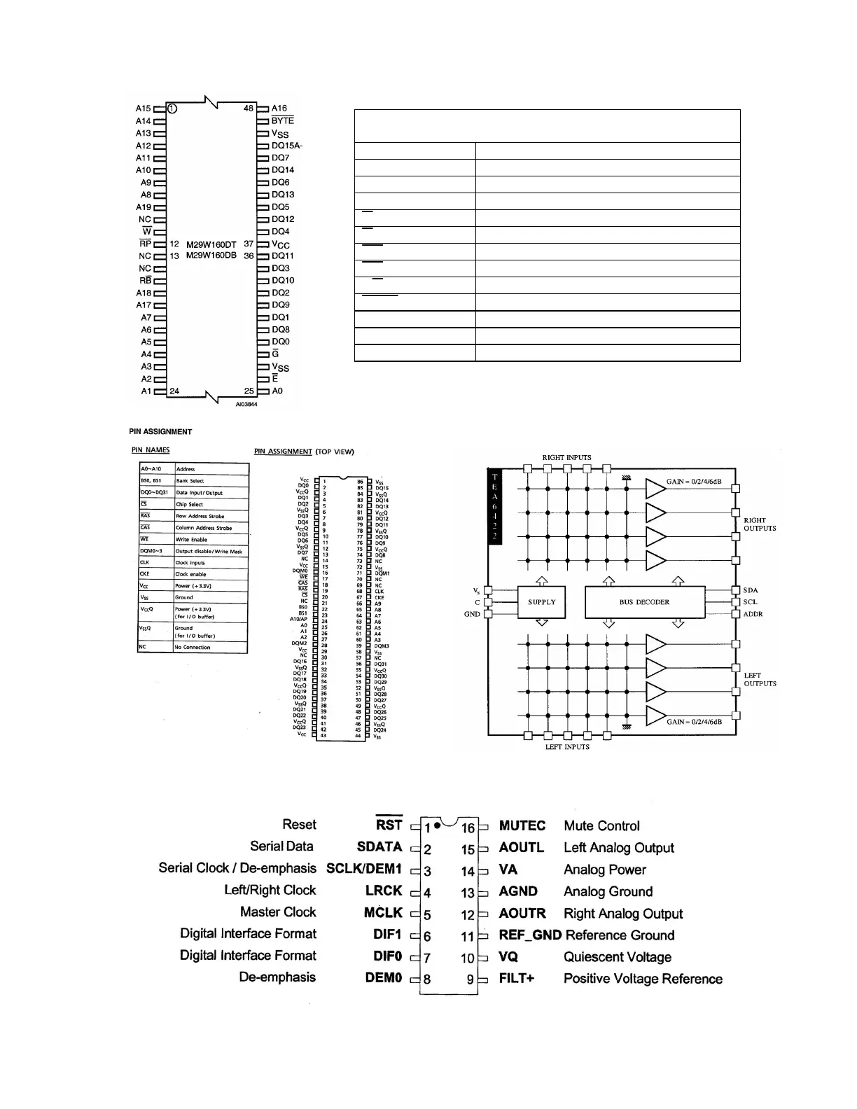
64
Signal Names
A0-A19 Adress Inputs
DQ0-DQ7 Data Inputs/Outputs
DQ8-DQ14 Data Inputs/Outputs
DQ15A-1 Data Input/Output or Address Input
E Chip Enable
G Output Enable
W Write Enable
RP Reset/Block Temporary Unprotect
RB Ready/Busy Output
BYTE Byte/Word Organization Select
VCC Supply Voltage
VSS Ground
NC Not Connected Internally
U2, FLASH, 16M, 3.3V TSSOP, 90NS
U3, SDRAM, 64MBIT, 2MX32, 3.3V
U201, AUDIO MATRIX, S028
U202, U503, CS4340-KS, DAC, 96 kHz, 3-5V
Integrated Circuit Diagrams
 Loading...