— 10 —
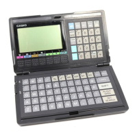
6. LSI, IC (Pin function)
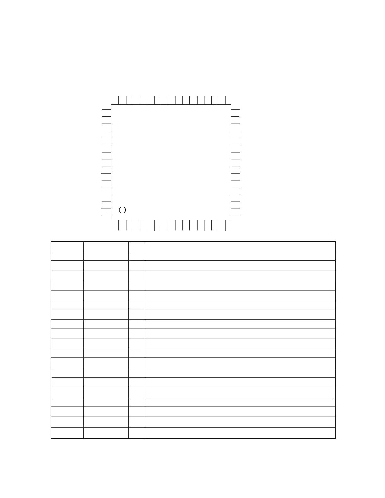
6-1. CPU: µPD 3056G-007 (LSI 1)
48 47 46 45 44 43 42 41 40 39 38 37 36 35 34 33
32
31
30
29
28
27
26
25
24
23
22
21
20
19
18
17
49
50
51
52
53
54
55
56
57
58
59
60
61
62
63
64
µPD 3056G-007
1 2 3 4 5 6 7 8 9 10 11 12 13 14 15 16
Pin No. Signal I/O Function
1 ~ 8 P0 ~ 7 I/O PORT P0: I/F output P1: I/F input
9 VSS I GND (0V)P6, P7: For buzzer
10 XI I Clock input
11 TSB Test Terminal
12 X0 O Clock output
13 VDD2 O
Internal power supply terminal
Power OFF: 0V ON: 5V
14 VDD1 I Power supply terminal (+5V)
15 FI I Internal clock terminal
16 FO O Internal clock terminal
17 SW I Main switch signa Power ON: 0V OFF: 5V
18 ISW I Sub switch signal Power ON: 0V OFF: 5V
19 ~ 21 CS1 ~ 3 O Enable signal for RAM
22 FE O Enable signal for ROM
23 WE O Write enable signal for RAM
24 CKO O Clock signal for LCD driver (NM360)
25 ~ 32 IO0 ~ 7 I/O Data bus
33 ~ 48 A0 ~ 15 O Address bus
49 ~ 63 KAC ~ K14 Key signal from keyboard
64 INT I Interrupt terminal
 Loading...