— 12 —
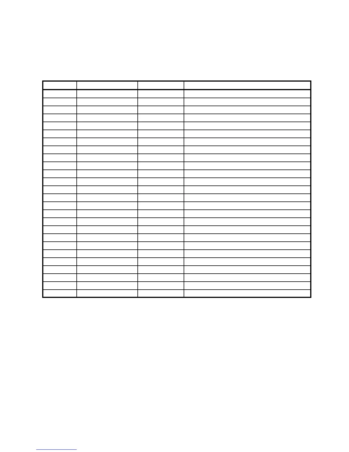
Pin No. Pin Name Input/Output Function
1 CSRA1 O Control for EL driver
2 CSRA2 O Chip selecting signal for RAM
4 WEB O Write enable signal for RAM
5 ~ 21 RA16,RA15,A14 ~ A0 O Address bus
22 ~ 29 IO7 ~ IO0 I / O Data bus
30 ~ 45 KY15 ~ KY0 I Key input signal
46 SW I Detection si
nal for battery cover
48 DN O Serial data output
50 SOUTB O Control for serial data output
51 SIN I Serial data input
52 VDD I Power supply to digtal circuit
53 TEST — TEST terminal
54 VTM O Voltage for the intenal circuit of CPU
55 OSC0 I Clock for CPU
56 OSC1 O Clock for CPU
57 GND — GND
58 ~ 61 V4 ~ V1 O Bias volta
e to LCD
62 INT0 I Control for forced power off
63 STNT I Control for VLCD
64 VLCD I Power supply to LCD
65 ~ 160 S95 ~ S0 O LCD driver signal (common)
161 ~ 193 C32 ~ C0 O LCD driver signal (segment)
194 GND — GND
195 BZ1 O Buzzer si
nal output
196 BZ2 O Buzzer si
nal output
197 VDD I Power suply to digital circuit
6. PIN FUNCTION
CPU µPD3058Ap-009 : COB (Chip on Board)
NOTE: The CPU is bonding on the PCB. If the CPU is defective, replace the PCB ASSY (A140745)
because the CPU cannot be replaced.
 Loading...