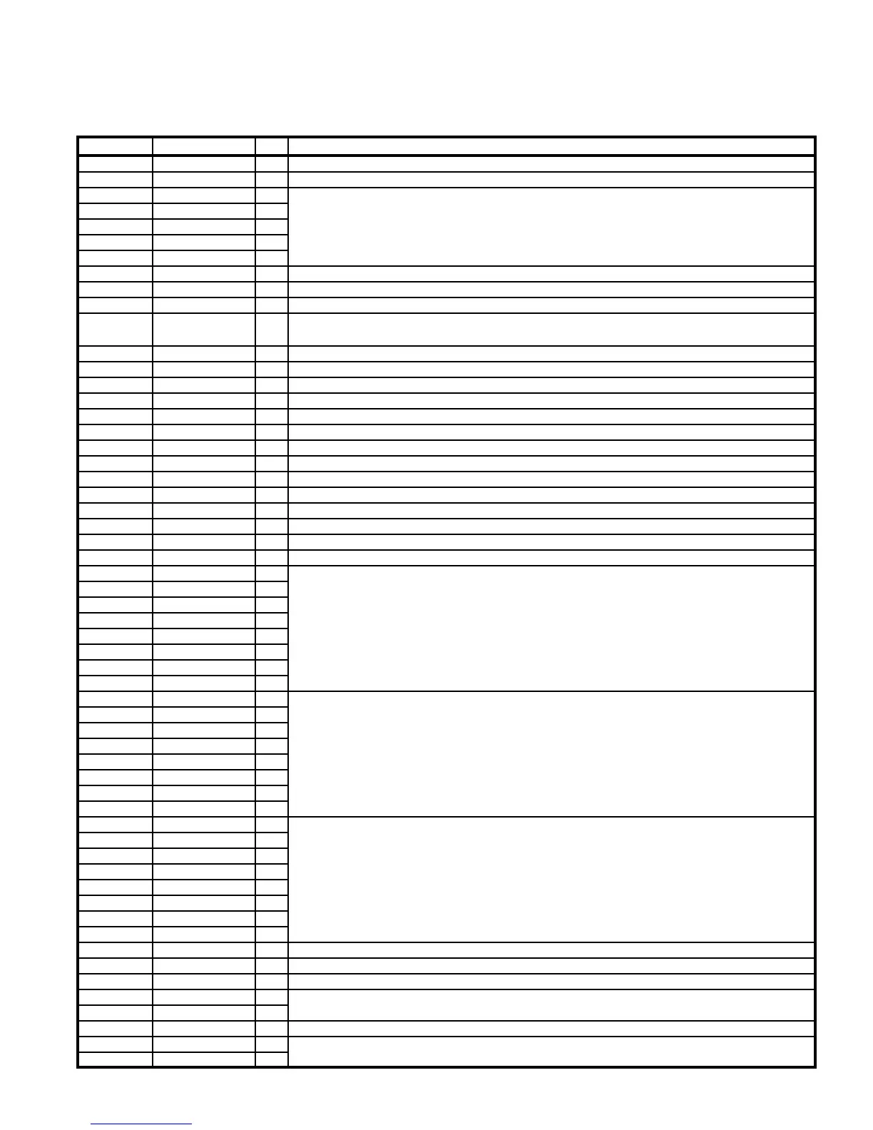
— 26 —
Pin No. Name I/O Function
1 VDD I Power suppl
for this CPU
2~65 S1~48,C1~16 O Common si
nals to LCD
66 V1 O
67 V2 O
68 V3 O Bias power suppl
to LCD
69 V4 O
70 V5 O
71 VLCD O Power suppl
to LCD
78 VSS — Ground for this CPU
80 P41 O Clock for LCD driver LSI
U2, U3:LC868900
82 P43 O
Signal to LCD driver LSI(U2, U3:LC868900)(AC voltage is supplied to LCD by this
si
nal.
84 P46 O Read si
nal to RAM
U42
U62
and LCD driver LSI
U2
U3:LC868900
85 P47 O Write si
nal to RAM
U42
U62
and LCD driver LSI
U2
U3:LC868900
87 P71 I Detection of low batter
volta
e
=2.5V
from IC
U2:S80725
90 P10 O Serial data output to another unit or a personal computer
91 P11 I Serial data input from another unit or a personal computer
93 P13 O
Control si
nal to power suppl
IC
DC/AC inverter IC
for EL
H: EL-OFF/L: EL-ON
96 P16 O Control si
nal for buzzer
H: buzzer-ON/L: buzzer-OFF
98 P57 O Chip select to LCD driver LSI
U3:LC868900
99 P56 O Chip select to LCD driver LSI
U2:LC868900
101 P54 O Clock to IC
U8:74HC273
for the ke
board data latch
102 P53 O Control si
nal to LCD driver LSI
U2, U3:LC868900
104 P51 O Address bus to RAM
U42, U62
105 P50 O Address bus to ROM
U5
106 VDD1 O Power suppl
for this CPU
107 P30 I
108 P31 I
109 P32 I
110 P33 I Si
nals for ke
assi
n from ke
board
111 P34 I
112 P35 I
113 P36 I
114 P37 I
115 P00 I/O
116 P01 I/O
117 P02 I/O
118 P03 I/O Address bus to the address data latch IC
U7:74HC373
119 P04 I/O
120 P05 I/O
121 P06 I/O
122 P07 I/O
123 P20 O
124 P21 O
125 P22 O
126 P23 O Address bus to ROM
U5
and RAM
U42, U62
127 P24 O
128 P25 O
129 P26 O
130 P27 O
131 ADLC O Control si
nal to the address data latch IC
U7:74HC373
132 -EROE O Chip select to ROM
U5
133 -RST I Reset si
nal for this CPU and LCD driver LSI
U2, U3:LC868900
134 XT1 I Timer clock for this CPU
135 XT2 O
136 VSS — Ground for this CPU
137 CF1 I Main clock for this CPU
138
2
7. LSI PIN FUNCTION
CPU (LC868016A): U1
 Loading...