EasyManua.ls Logo

Clarion PF-2945A-A User Manual

Clarion PF-2945A-A
28 pages
To Next Page IconTo Next Page
To Previous Page IconTo Previous Page
Page #27 background image
To P602 of Main PWB(B1) (page 25)
CIRCUIT DIAGRAM 9/10
Switch PWB(B2) section
-27-
PF-2945A-A/PF-2982B-A
J1---11,12, 18Pin
IC1---20Pin
IC2---66,67Pin
IC2---68Pin
IC2---63,64Pin
IC1---18,19Pin
J1---13,16,17Pin
J1---15Pin
IC1---1,2,3,4,5,6,
7,8,9,10,Pin
Waveform
Waveform
point
C03
C04
D03
Waveform Waveform
Waveform
point
Waveform point
C05
IC1---17Pin
VOLUME
POWER
TUNE
EJECT
TONE
IC2---1~52Pin
IC2---53~60Pin
IC2---71~78Pin
IC2---79~100Pin
B04
D02
A01
P
Q
T
S
S
L
M
N
U
F
E
D
C
B
A
I
K J
G
A
B
C D
E
F
J
I
K
O
P
Q
H
L
M
N
R
S
T
U
V
KEY NAME
A
B
C
D
E
F
G
H
I
J
K
L
M
N
O
P
Q
R
S
T
V
U
1
2
3
4
5
6
EJECT
--------
CD/AUX
FM/AM
SAT
TEXT
RPT/RDM
SCAN
POWER/VOLUME
PTY/CAT
SEEK DOWN
SEEK UP
FOLDER UP
FOLDER DOWN
MENU
TB/TUNE
MARK
CD INSERT L
CD INSERT L
Question and Answer IconNeed help?

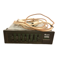
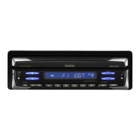
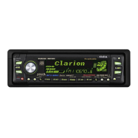
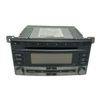
Do you have a question about the Clarion PF-2945A-A and is the answer not in the manual?

Clarion PF-2945A-A Specifications

General IconGeneral
BrandClarion
ModelPF-2945A-A
CategoryCar Receiver
LanguageEnglish

Summary

PRODUCT SPECIFICATIONS

Tuner & CD Specifications

Technical details for tuner reception and CD playback operations.

Audio & Operations Specs

Specifications for AUX input, MP3/WMA, general unit parameters, and audio output.

Component Listing

Lists the main component groups of the car stereo unit.

IMPORTANT NOTES AND CAUTIONS

General Notes

Important product notes, disclaimers, and media compatibility information.

Repair and Inspection Guidelines

Instructions and precautions for engineers performing repairs or inspections.

Safety Precautions

Essential safety warnings regarding operation, handling, and repairs.

ADJUSTMENTS AND IC EXPLANATION

Adjustment Procedure

Step-by-step guide for calibrating the unit's tuner and settings.

IC Pin Descriptions

Detailed function of each pin for the ICs used in the system.

SYSTEM BLOCK DIAGRAM

CD Mechanism Block Diagram

Visual representation of the CD mechanism's internal structure and connections.

MAIN SECTION OVERVIEW

Main PWB and Connectivity

Overview of the main Printed Wiring Board and its external connections.

EXPLODED VIEW AND PARTS LIST

Escutcheon Section Parts

Illustrated parts list for the unit's front panel assembly (Escutcheon).

MAIN SECTION PARTS LIST

Main PWB Components

Detailed list of parts mounted on the main Printed Wiring Board.

CD MECHANISM ASSEMBLY

CD Mechanism Exploded View

Detailed exploded view of the CD mechanism showing all parts.

ELECTRICAL PARTS LIST

Main PWB Electrical Components

Comprehensive list of electronic components for the Main PWB.

PRINTED WIRING BOARD SECTIONS

PWB Parts Lists

Parts lists for Switch, Sub, CD, and Sensor Printed Wiring Boards.

SYSTEM CONNECTIONS

Connector Pinouts and Overview

Details of Main, SIE-BUS, AUX connectors and system interconnection diagram.

PRINTED WIRING BOARD - SUB PWB(B3)

Sub PWB(B3) Layouts

Component and solder side layouts for the Sub PWB(B3).

PRINTED WIRING BOARD - MAIN PWB(B1) 1/7

Main PWB(B1) Layouts 1/7

Component and solder side layouts for the Main PWB(B1), part 1 of 7.

PRINTED WIRING BOARD - MAIN PWB(B1) 2/2

Main PWB(B1) Solder Side 2/2

Solder side layout for the Main PWB(B1), part 2 of 2.

PRINTED WIRING BOARD - SWITCH PWB(B2) 1/2

Switch PWB(B2) Component Side

Component side layout for the Switch PWB(B2), part 1 of 2.

PRINTED WIRING BOARD - SWITCH PWB(B2) 2/2

Switch PWB(B2) Solder Side

Solder side layout for the Switch PWB(B2), part 2 of 2.

CIRCUIT DIAGRAM - SUB PWB(B3)

Sub PWB(B3) Circuit Diagram

Schematic diagram illustrating the circuit of Sub PWB(B3).

CIRCUIT DIAGRAM - MAIN PWB(B1) 1/7

Main PWB(B1) Circuit Diagram 1/7

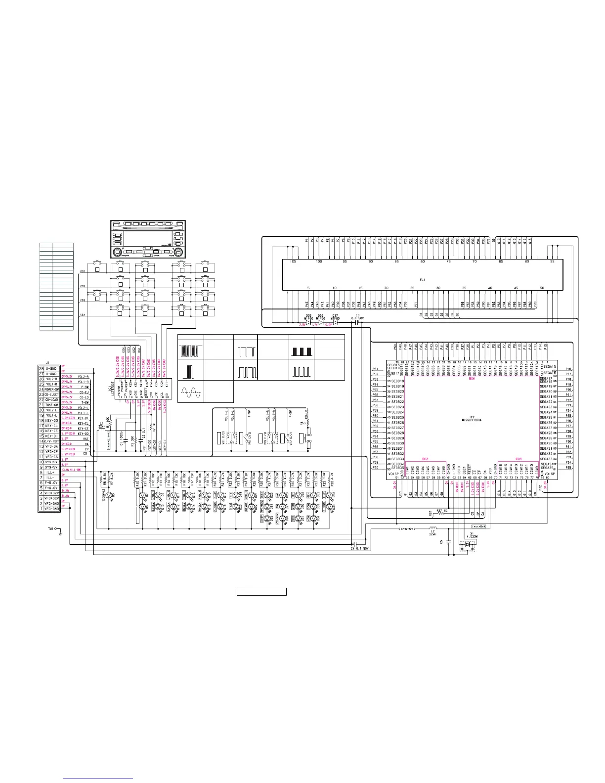
Schematic diagram of the Main PWB(B1), part 1 of 7.

CIRCUIT DIAGRAM - MAIN PWB(B1) 2/7

Main PWB(B1) Circuit Diagram 2/7

Schematic diagram of the Main PWB(B1), part 2 of 7.

CIRCUIT DIAGRAM - MAIN PWB(B1) 3/7

Main PWB(B1) Circuit Diagram 3/7

Schematic diagram of the Main PWB(B1), part 3 of 7.

CIRCUIT DIAGRAM - MAIN PWB(B1) 4/7

Main PWB(B1) Circuit Diagram 4/7

Schematic diagram of the Main PWB(B1), part 4 of 7.

CIRCUIT DIAGRAM - MAIN PWB(B1) 5/7

Main PWB(B1) Circuit Diagram 5/7

Schematic diagram of the Main PWB(B1), part 5 of 7.

CIRCUIT DIAGRAM - MAIN PWB(B1) 6/7

Main PWB(B1) Circuit Diagram 6/7

Schematic diagram of the Main PWB(B1), part 6 of 7.

CIRCUIT DIAGRAM - MAIN PWB(B1) 7/7

Main PWB(B1) Circuit Diagram 7/7

Schematic diagram of the Main PWB(B1), part 7 of 7.

CIRCUIT DIAGRAM - SWITCH PWB(B2)

Switch PWB(B2) Circuit Diagram

Schematic diagram illustrating the circuit of the Switch PWB(B2).

PRINTED WIRING BOARD - SENSOR/CD PWB

Sensor/CD PWB Layouts

Component and solder side layouts for Sensor and CD PWBs.

CIRCUIT DIAGRAM - SENSOR/CD PWB

Sensor/CD PWB Circuit Diagram

Schematic diagram illustrating the circuit of Sensor and CD PWBs.

Related product manuals