

J
Justin RussellAug 12, 2025
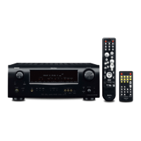
What to do if Denon Receiver remote control is not working?
- CCourtney TorresAug 12, 2025
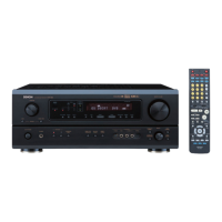
If your Denon Receiver isn't responding to the remote, here are a few things to check: * Make sure the batteries aren't dead and replace them if needed. * Ensure you're close enough to the unit. * Remove any obstacles blocking the remote's signal. * Verify you're pressing the correct button. * Check that the batteries are inserted with the correct polarity.