35
Using BIOS
Advanced Chipset Features
These items define critical timing parameters of the motherboard. You should leave
the items on this page at their default values unless you are very familiar with the
technical specifications of your system hardware. If you change the values incor-
rectly, you may introduce fatal errors or recurring instability into your system.
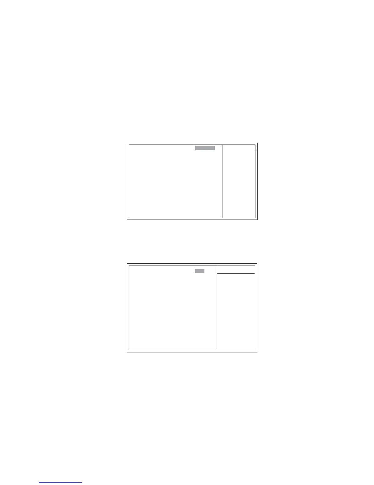
: Move Enter: Select +/-/PU/PD:Value F10:Save ESC:Exit F1: General Help
F5:Previous Values F6:Fail-Safe Defaults F7:Optimized Defaults
Phoenix-Award WorkstationBIOS CMOS Setup Utility
Advanced Chipset Features
DRAM Configuration [Press Enter]
LDT & PCI Bus Control [Press Enter]
PCIE GFX Core Payload Size [64 Bytes]
PCIE GPP Core Payload Size [64 Bytes]
GFX0 Link Width [x16]
UMA Frame Buffer Size [256MB]
Current UMA Size 256MB
AGP Aperture Size [128MB]
GFX Clock Mode [Sync]
Async GFX Clock 200MHz
Async GFX Clock Source 14.318MHz OSC
MCLK Spread Spectrum Disabled
Dynamic CKE [Enabled]
Video Display Devices [Auto]
Tv Standard [NTSC]
NB Azalia [Enabled]
System BIOS Cacheable [Disabled]
Item Help
Menu Level
DRAM timing and
control
x
x
x
DRAM Configuration
Scroll to this item and press <Enter> to view the following screen:
(Press Enter)
Item Help
Menu Level
Phoenix-Award WorkstationBIOS CMOS Setup Utility
DRAM Configuration
x
Timing Mode Auto
Memclock index value or Limi DDR2 400
SPD Checksum Restart [Ignore]
DQS Training Control [Perform DQS]
CKE base power down mode [Disabled]
CKE based powerdown [Per channel]
Memclock tri-string [Disabled]
Memory Hole Remapping [Enabled]
Auto Optimize Bottom IO [Enabled]
Bottom of [31:24] IO space D0
Bottom of UMA DRAM [31:24] [FC]
F5:Previous Values F6:Fail-Safe Defaults F7:Optimized Defaults
: Move Enter: Select +/-/PU/PD:Value F10:Save ESC:Exit F1: General Help
x
 Loading...