ESMT
Preliminary F49L320UA/F49L320BA
Elite Semiconductor Memory Technology Inc. Publication Date : Jan. 2008
Revision: 0.4 2/54
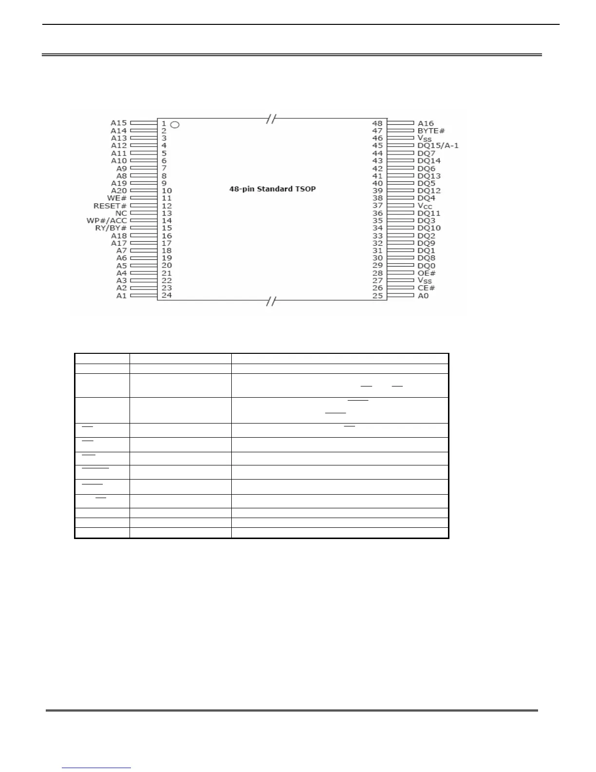
4. PIN CONFIGURATIONS
4.1 48-pin TSOP
4.2 Pin Description
Symbol Pin Name Functions
A0~A20 Address Input To provide memory addresses.
DQ0~DQ14 Data Input/Output
To output data when Read and receive data when Write.
The outputs are in tri-state when
OE or CE is high.
DQ15/A-1
Q15 (Word mode) /
LSB addr (Byte Mode)
To bi-direction date I/O when
BYTE is High
To input address when
BYTE
is Low
CE
Chip Enable
To activate the device when CE is low.
OE
Output Enable To gate the data output buffers.
WE
Write Enable To control the Write operations.
RESET
Reset Hardware Reset Pin/Sector Protect Unprotect
BYTE
Word/Byte selection input To select word mode or byte mode
RY/ BY
Ready/Busy To check device operation status
V
CC
Power Supply To provide power
GND Ground
NC No connection
AVR3600 harman/kardon
 Loading...