3-5-5
LOOP
FILTER
(V«PLL
AND
U*PLL
UNITS)
A
loop filter
converts the
phase-detected signal
(pulse
signal) to DC voltage
(PLL lock
voltage) to control the VCO
oscillating signal.
The PLL lock
voltage changes
the
reactance of a
varactor diode in
the VCO circuit. The
DC
voltage of the
VHP PLL is also
used for the receiver
tuning
circuit.
The
phase-detected
signal output from the PLL 1C
(pin
13)
passes
through the
charge pump control
(IC2) and is applied
to
the following
loop filter:
For VHF PLL :
Lag-read-type loop filter
(R2, R3. C5, C6)
ForUHFPLL :
Active loop
filter
(Q4.
Q5.
R10~R12.
C15~C17)
The
charge pump control
(IC2) cuts off the line
of
IC1
and
the loop
filter while In the
circuit off condition of the
power
saver
function.
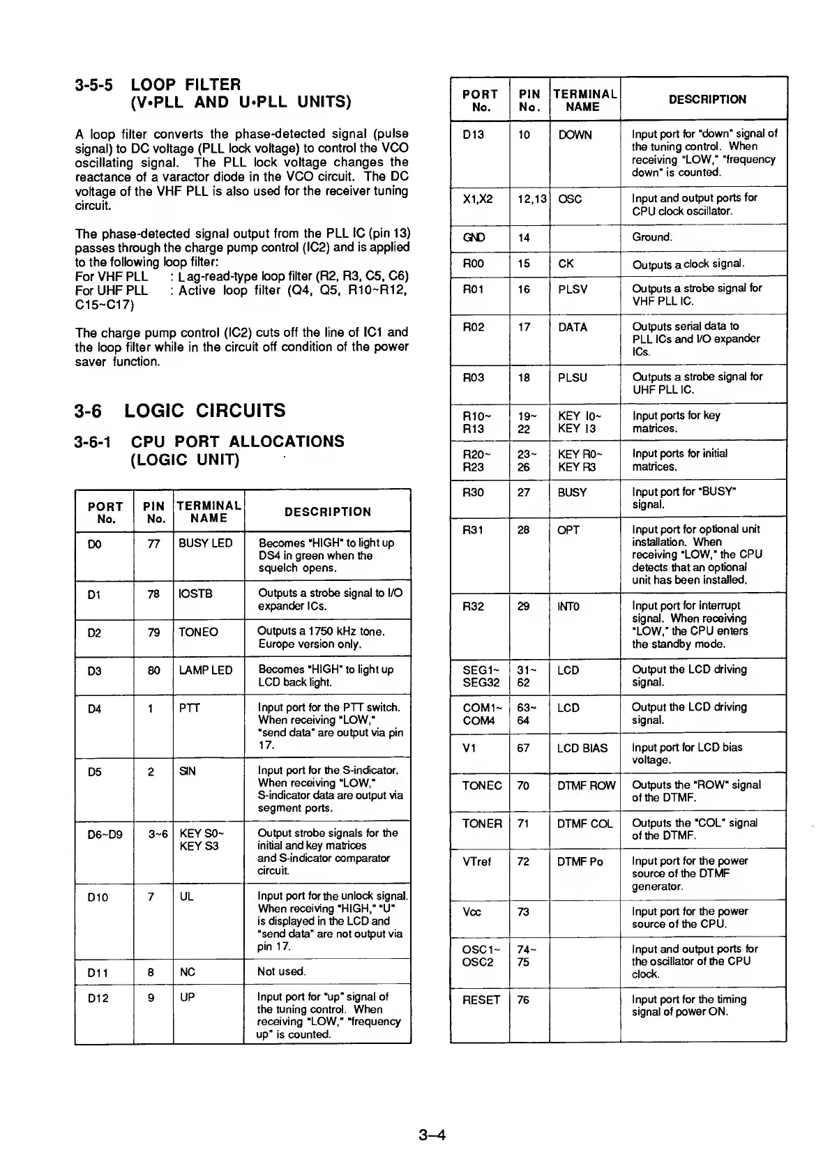
3-6
LOGIC
CIRCUITS
3-6-1
CPU
PORT
ALLOCATIONS
(LOGIC
UNIT)
PORT
No.
PIN
No.
TERMINAL
NAME
DESCRIPTION
DO
77
BUSY LED
Becomes “HIGH" to
light up
DS4 in
green
when the
squelch
opens.
D1
78
lOSTB
Outputs a
strobe
signal to I/O
expander ICs.
D2
79
TONEO
Outputs
a
1 750 kHz tone.
Europe version
oniy.
D3
80
LAMP
LED
Becomes “HiGH" to iight up
LCD back iight.
D4
1
PTT
input
port for the PTT switch.
When receiving “LOW."
“send data" are output via pin
17.
D5
2
SIN
input port for the S-indicator.
When receiving
“LOW,"
S-indicator data are output via
segment ports.
D6-D9
3-6
KEY SO-
KEY S3
Output
strobe signals for
the
initial and key matrices
and S-indicator comparator
circuit.
D10
7
UL
input port for
the
uniock signal.
When
receiving "HIGH,"
"U"
is
displayed
in the LCD and
“send data" are not output via
pin 17.
Dll
8
NC
Not used.
D12
9
UP
Input port for “up" signal of
the
tuning
controi. When
receiving “LOW," “frequency
up”
is
counted.
PORT
No.
PIN
No.
TERMINAL
NAME
DESCRIPTION
D13 10
DOWN
Input
port for
“down"
signal of
the
tuning
control. When
receiving
“LOW,”
“frequency
down" is
counted.
XI,X2
12,13 OSC
Input
and
output ports
for
CPU
clock
oscillator.
GND 14
Ground.
ROO 15
CK
Outputs a
clock
signal.
R01 16
PLSV
Outputs a
strobe
signal for
VHF
PLL 1C.
R02 17
DATA
Outputs
serial
data to
PLL
ICs
and I/O
expander
ICs.
R03
18
PLSU
Outputs a
strobe
signal for
UHFPLLIC.
RIO-
R13
19-
22
KEY
10-
KEY
13
Input ports
for key
matrices.
R20-
R23
23-
26
KEYRO-
KEYR3
Input ports for initial
matrices.
R30 27
BUSY
Input port
for “BUSY"
signal.
R31 28
OPT
Input port for
optional unit
installation.
When
receiving “LOW," the CPU
detects that an
optional
unit has been
installed.
R32 29 INTO
Input port for interrupt
signal. When receiving
“LOW," the
CPU enters
the
standby mode.
SEG1-
SEG32
31-
62
LCD
Output the LCD driving
signal.
COM1-
COM4
63-
64
LCD
Output
the LCD driving
signal.
VI 67
LCD BIAS
Input port for LCD
bias
voltage.
TON
EC
70
DTMF
ROW
Outputs the “ROW"
signal
of the DTMF.
TONER
71
DTMF COL
Outputs the “COL”
signal
of the DTMF.
VTref
72
DTMF Po
Input port for the
power
source of the DTMF
generator.
Vcc 73
Input port for
the power
source of the CPU.
OSC1-
OSC2
74-
75
Input and output
ports for
the
oscillator of the CPU
clock.
RESET 76
Input port for the
timing
signal of power ON.
3-4

 Loading...