While no CW transmit
IF signal exists,
Q39
and
Q23
turn
the
switching diode (D35)
OFF to ensure
transmit
isolation.
4-2-9
OUTPUT POWER
METER CIRCUITS
(MAIN
UNIT)
The “FOR”
voltage
from the PA UNIT
is applied
to the Po
meter
amplifier
(1010
pin
3)
and then to
the meter.
R189
and
0261 are used
for peak power measurement.
4-2-10
T/R
SWITCHING
CIRCUIT
(MAIN UNIT)
When
the PTT or [TRANSMITl
switch is
set to
transmit,
IC13
pin
10
and
1013
pin
3
are “LOW.” At this time,
049
turns ON, and 0
V is present on the “R8” voltage line.
050
turns OFF, and
there is
8
V present on the “T8”
voltage
line.
When the PTT or
[TRANSMIT] switch is
set to receive,
1013
pin 10 and
1013
pin 3
are “HIGH.” At this
time,
049
turns OFF, and 8
V Is present on the “R8” voltage
line. 050
turns ON, and
there-is 0 V present on the
“T8” voltage
line.
When PLL data or
the operating mode
is
changed, the
“DNB” signal
line becomes “LOW,” turning OFF the T8
—
preventing unwanted transmission.
4-3
PLL
CIRCUITS
4-3-1
GENERAL
DESCRIPTION
The PLL
UNIT
generates
a 1st LO signal
(70.951
5~
100.4515 MHz
variable) and 2nd LO
signal
(61.44 MHz
fixed) used in
the MAIN UNIT.
The
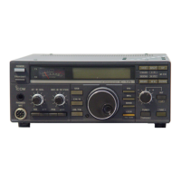
10-725
uses
a dual loop
PLL system.
A main loop PLL uses
4 VOO circuits for
all HF band
coverage within 512 kHz
steps.
A sub loop
PLL uses a
DOS (Direct
Digital Synthesizer)
system
for
512 kHz coverage
within 10 Hz steps.
The DDS system
provides
a
rapid
lockup
time and
high quality frequency
oscillation.
4-3-2
REFERENCE
OSCILLATOR CIRCUIT
(PLL
UNIT)
A 30.72 MHz
reference
frequency is produced
by
the
oscillator 033 and
X2. The
reference frequency, buffer-
amplified at
034,
is
divided by 2 at 1015 and is then
applied
to
the PLL
circuit
as
the PLL reference frequency.
The signal oscillated at 033
is multiplied
by
2 at Q36.
The
resulting
61.44
MHz
signal is
filtered
at the bandpass
filter and is
then applied to the
MAIN UNIT via
P4 as
the
2nd LO
signal.
4-3-3
MAIN LOOP
(PLL UNIT)
The
main loop uses a
PLL
10 (1013)
which contains a
programmable
divider, phase
detector,
data
shift register
and data latch
circuits. The
main
loop generates
70.951
5~1
00.451
5
MHz
signals in 512 kHz
steps.
Because the sub loop produces 10 Hz steps,
the PLL
produces a 30 MHz frequency
range in 10
Hz
steps.
The oscillated signal at one of
the
4 VOOs
(015,
017,
019,
021
;
see Section
4-3-4
for details) is
amplified at 023.
The
signal
is mixed with the
sub loop
output
(fm:
62.05~62.561
99
MHz)
at
1016. 023 is an isolator
which
ensures
that the
mixer input
does not affect
the VCO
output.
The mixed
signal
is
amplified
at 027 and is
then filtered
at the low-pass
filter (L23~L25,
092,
C93, C99~C103).
The filtered signal, amplified at
026,
is divided by
4
at
1014
and is
then
applied to the PLL
10
(IC13).
The
phase of the divided signal at IC14, detected at
the PLL
10
(1013)
using
a
reference frequency
(fpEp)
of
512
kHz,
is
then
output
from pin
17.
The 512 kHz
frequency is obtained
from
the
reference oscillator
(033).
30.72
MHz
oscillated
at
033,
is divided
by 2
at IC15
and
divided by 30 at the programmable divider section of IC13.
The phase detected signal is
then
converted to
the lock
voltage
at the
loop filter
(Q12~Q14),
and applied to
the
VCO. Thus, the VCO output (PLL output) is
locked
to
produce
stable oscillation.
The PLL oscillation frequency
is
obtained by the following
calculation:
fv
=
fLO
+
NTXfREF
fv
:
Main
loop output
fto
: Sub loop output
Nt
:
Dividing ratio from the CPU
ffiEp:
Reference frequency
(512
kHz)
4-3-4
VCO CIRCUIT (PLL UNIT)
The transceiver’s C/N ratio
is
determined
by
the VCO
and
the
loop filter. 4
VCO
circuits keep the low noise
and
reduce
spurious emissions.
016,
018,
020 and 022
are
VCO
switches
which
select the operating VCO
with
“VC01 ”~“VC04” lines.
4-3-5
SUB
LOOP
(PLL UNIT)
The
sub loop uses the DDS system that
generates
62.05~62.561
99
MHz signals in 10 Hz steps.
The oscillated signal
at
the
VCO
(029)
is
buffer-amplified at
030
and
mixed with the 2nd
LO
signal (61.44
MHz) at
IC17. The resulting signal
passes
through the low-pass
filter, is amplified
at
032,
and
is then applied to the DDS
UNIT.
The output pulse-type signal from the DDS
UNIT passes
through the loop filter (R133, R134,
C114,
C115,
L42)
where it is converted into
a DC
signal (lock voltage).
The
lock voltage is applied to
the
VCO
to
lock the
oscillating
frequency.
4
—
6

 Loading...