3-1-8 AF CIRCUIT (MAIN UNIT)
The AF circuit drives the speaker.
AF signals from the detector circuit are selected at the AF
selector (IC5002), and are passed through the AF filter
(Q5026, Q5005) and volume control (R5082).
The signals are amplifi ed at the AF power amplifi er (IC5003)
to a level needed to drive the speaker (SP3001).
3-1-9 AGC CIRCUIT (MAIN UNIT)
The AGC (Automatic Gain Control) circuit reduces signal
fading and keeps the audio output level constant.
AF signals from the AM detector circuit (Q5004) are
converted into DC voltage at integral circuits (R5030/C5026,
R5105/C5025), and are then applied to inversion amplifi ers
(Q5010/Q5031).
These amplifiers reduce the amplifier gain of IF amplifiers
(Q5002, Q5003, Q4003) and the RF amplifi er (Q4001) while
receiving a strong signal.
3-1-10 VOR CIRCUIT (LOGIC UNIT) [IC-A22/E only]
The VOR circuit detects a variable signal (VORC) and
reference signal (VORS) from a VOR station. The VOR
circuit sends these signals to the CPU (IC6001).
When the transceiver is set in the navigation band (108.000–
117.975 MHz), the NAV port (IC6001, pin 43) becomes
“HIGH” turning the VOR circuit ON via Q6108. Q6108
controls a 5 V power source for the VOR circuit.
The signal from the AM detector (DETO) is buffer amplifi ed
at the buffer amplifi er (IC6105b).
The DETO signal includes 30 Hz variable phase components
and 9960 Hz reference phase components.
The 30 Hz component passes through the 30 Hz bandpass
fi lter (IC6105d), and is converted to a square-wave signal at
the VORC comparator (IC6108a). The square-wave signal is
then applied to IC6001 (pin 28) as a variable signal (VORC).
The 9960 Hz component passes through the 10 kHz
bandpass filter (IC6105c). These components are FM
modulated with 480 Hz deviation and 30 Hz modulation.
Signals are then amplifi ed at a limiter amplifi er (IC6106a),
and detected at an FM detector (IC6106b) to obtain a 30 Hz
reference signal.
The 30 Hz signal is compensated on phase at IC6107a. This
signal is passed through the 30 Hz low-pass fi lter (IC6107b)
and is converted to a square-wave signal at the VORS
comparator (IC6108b). This signal is applied to IC6001 (pin
27) as a reference signal (VORS).
A portion of output from IC6105c is applied to the VOR
sensor (Q6109, Q6110). When VOR signal level is low, the
output from IC6105c is reduced. Q6110 cannot be turned
ON, then IC6001 (pin 29) receives “HIGH” to indicate “OFF
FLAG” indicator.
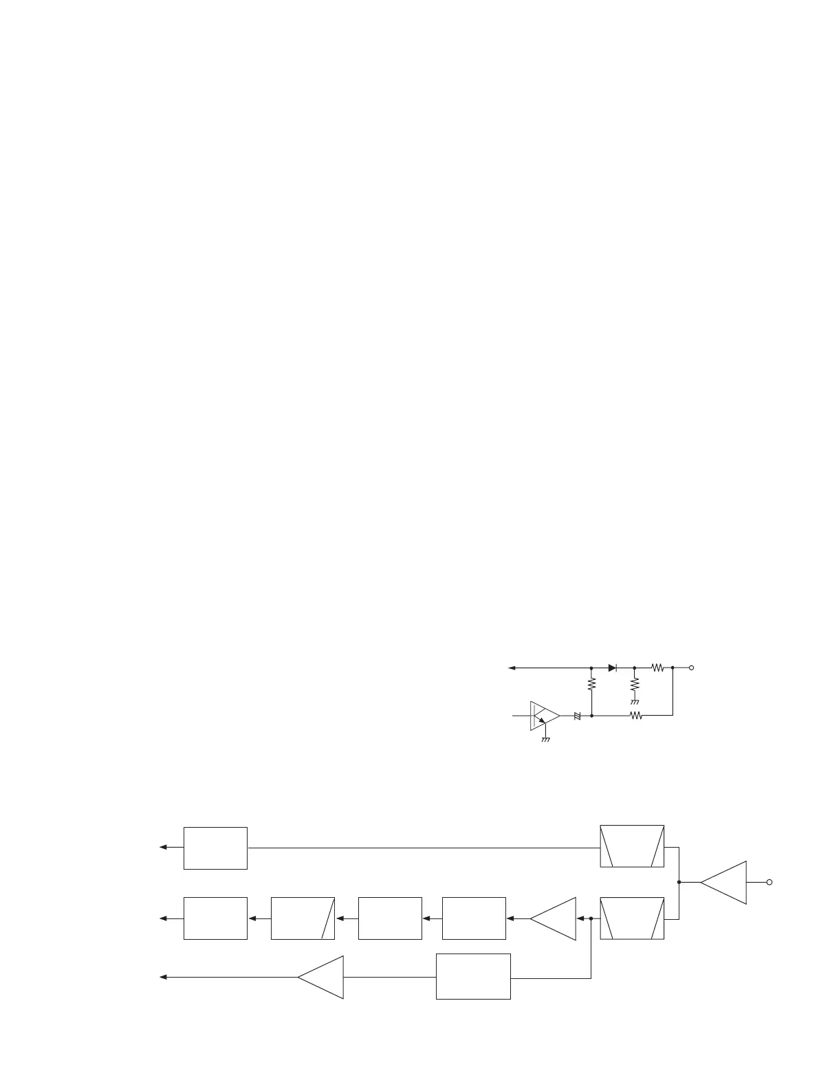
3-1-11 ANL CIRCUIT (MAIN UNIT)
The ANL (Automatic Noise Limiter) circuit (D5003, Q5008,
R5015–R5018) reduces pulse noises.
The AM detector output signal (DETO) from Q5004 is
applied to the cathode of D5003 passing through R5015
where it is divided by R5015 and R5016. The DETO signal is
also applied to the anode of D5003, passing through R5017
and R5018.
When the ANL function is activated (Q5008 is ON), C5024
is grounded. The detector output, including pulse noise, is
applied to the cathode of D5003 only. If pulse noises are
received, the cathode voltage of D5003 becomes higher
than the anode voltage and D5003 turns OFF. Thus, while
pulse noises are received, the detected signal is not applied
to IC5002.
3 - 2
• VOR CIRCUIT BLOCK DIAGRAM
30 Hz
Inversion amp.
Q6110
30 Hz
10 kHz
DETO
VORC
to IC6001 pin 28
VORS
to IC6001 pin 27
VORO
to IC6001 pin 29
Limiter amp.
IC6106a
Buffer amp.
IC6105b
Comparator
IC6108a
LPF
IC6107b
Comparator
IC6108b
Phase shift
IC6107a
FM detector
IC6106b
VOR
sensor
Q6109, D6110
BPF
IC6105c
BPF
IC6105d
Q5008
D5003To IC5002
• ANL CIRCUIT
R5015
220 k
AF signal
from Q5004
R5016
100 k
R5018
100 k
R5017
330 k
+
C5024
 Loading...