3-2 TRANSMITTER CIRCUITS
3-2-1 MICROPHONE AMPLIFIER CIRCUIT (MAIN UNIT)
AF signals from the microphone or from the [MIC] jack are
applied to the ALC amplifi er (IC5004, pin 9) through R5047.
R5047 adjusts the microphone input level.
The output signal from IC5004 (pin 7) are amplified at the
buffer amplifi er (lC5005b) and low-pass fi lter (IC5005a). The
signal (MOD) is applied to the AM modulator (D4012) on the
RF unit.
When using a headset, the SIDET signal from Q4020
becomes “HIGH,” turning IC5008 ON. Then a portion of
amplified signal from IC5005b is applied to the AF power
amplifi er (IC5003) as a monitor signal.
3-2-2 MODULATION CIRCUIT (RF UNIT)
Using the MOD signal from the microphone amplifi er circuit,
the modulation circuit modulates Tx LO signal from the VCO.
During transmission, the LO signal from the VCO board
is output through buffer amplifiers (Q4004, Q4005) and
Tx/Rx switch (D4010). This signal is then applied to the AM
modulator (D4012).
Q4006 amplifi es the LO signal with a gain controlled by an
AF signal (MOD) to make low level modulation.
3-2-3 DRIVE/POWER AMPLIFIER CIRCUITS (RF UNIT)
The modulated RF signal from Q4006 is amplified by the
pre-drive amplifi er (Q4007) and the power amplifi er (IC4002)
in sequence to obtain 5 W (at 12 V DC) of transmit output
power. The amplifi ed signal is passed through the antenna
switching circuit (D4003) and low-pass fi lter (L4001–L4003,
C4001–C4005) and is then applied to the antenna connector
(J3001).
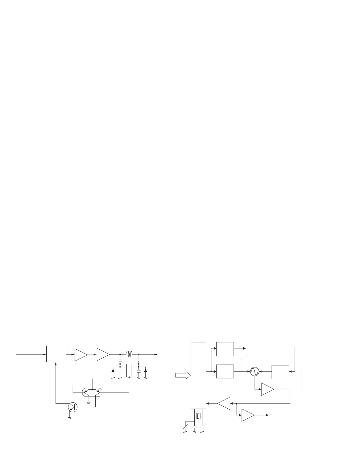
3-2-4 APC CIRCUIT (MAIN UNIT)
The APC circuit protects the power amplifi er (IC4002) from a
mismatched output load.
The APC detector circuit (D4005, D4004, L4006) detects
forward signals and rectified signals at D4005 and D4004
respectively. The combined voltage is at a minimum level
when the antenna is matched at 50
Ω
, and is increased
when it is mismatched.
The detected voltage is applied to one of the differential
amplifier input (Q4010) and a power setting voltage is
applied to the other input. When the antenna impedance is
mismatched, the detected voltage exceeds the APC output
current via Q4014 to decrease the output power.
The current of the APC attenuator (D4013) is controlled
by the APC circuit to protect the power amplifier from a
mismatched condition as well as stabilize the output power.
3-3 PLL CIRCUITS
3-3-1 GENERAL (RF UNIT)
A PLL circuit provides stable oscillation of the transmitting
frequency and the receiving frequency. The PLL output
frequency is controlled by the divided ratio (N-data) of the
programmable divider.
3-3-2 VCO CIRCUIT (VCO BOARD)
The VCO (Q7001, Q7002, D7001) employs an oscillation
circuit. Frequency shifting for transmitting (or weather
channel receiving) and receiving is performed by changing
the bias voltage of D7002.
LO signals generated by the VCO are amplifi ed at the buffer
amplifier (Q7003), and are then applied to the 1st mixer
(Q4002) or AM modulator (D4012) through buffer amplifi ers
(Q4004, Q4005) and Tx/Rx switch (D4010, D4021). Signals
from Q7003 are also applied to the PLL IC (IC4001) through
a buffer amplifi er (Q4015).
3-3-3 PROGRAMMABLE DIVIDER (RF UNIT)
Signals from Q4015 are input into the PLL IC (IC4001, pin 2),
and divided N times at the programmable divider section. The
divided signals are detected on phase at the phase detector
section using the reference frequency. The output signal
from the phase detector is passed through the charge pump,
and is output from pin 8.
The output signal (error pulse) from pin 8 passes through a
loop fi lter (R4064, R4065, C4102, C4104) and changes DC
voltage. This signal is applied to the VCO board as the PLL
lock voltage (LV).
The output signal from pin 8 is also applied to the BPF
control circuit (Q4018, D4019) to change the center
frequency of the receiver bandpass fi lters.
3 - 3
Differential amp.
Q4010
Reference
voltage
Current
controller
Pre-drive amp.
T +5
D4005 D4004
L4006
To
antenna
Q4014
Power amp.
APC
attenuator
D4013
RF signal from
buffer amp.
• APC CIRCUIT
Q4007
IC4002
BPF
control
PLL IC
IC4001
Data from
the CPU
• PLL CIRCUIT BLOCK DIAGRAM
Loop
filter
Shift
control
Buffer amp.
Buffer amp.
Buffer amp.
Q4004,
Q4005
Q4015
To 1st mixer (Q4002)
or AM modulator (D4012)
through Tx/Rx switch
(D4010, D4021)
Q7003
From the CPU
SHIFT
OUT
LV
Q4018
8
2
15 16
12.8 MHz
X4001
VCO
Q7001, Q7002
VCO
board
D7002
To Rx BPF
(D4006–D4009)
 Loading...