4 - 5
<OPERATION ON THE RIGHT BAND>
The modulation signals are applied to the variable capacitor
D87 of the left band VCO (Q73, D87, 91, 92) via the
modulation selector (IC63) and modulation mute switch
(Q64), and modulated. The modulated VCO output are
amplifi ed by the buffer (Q76) and LO amplifi er (IC45), and
applied to the transmit amplifi ers as the TX signal, via the
VCO switch (D102). The amplifi ed LO signals are applied to
the transmit amplifi ers via the LO switch (D103), two HPFs
(L124, C527, 532; L159, C533, 535) and attenuator (R43,
47, 57).
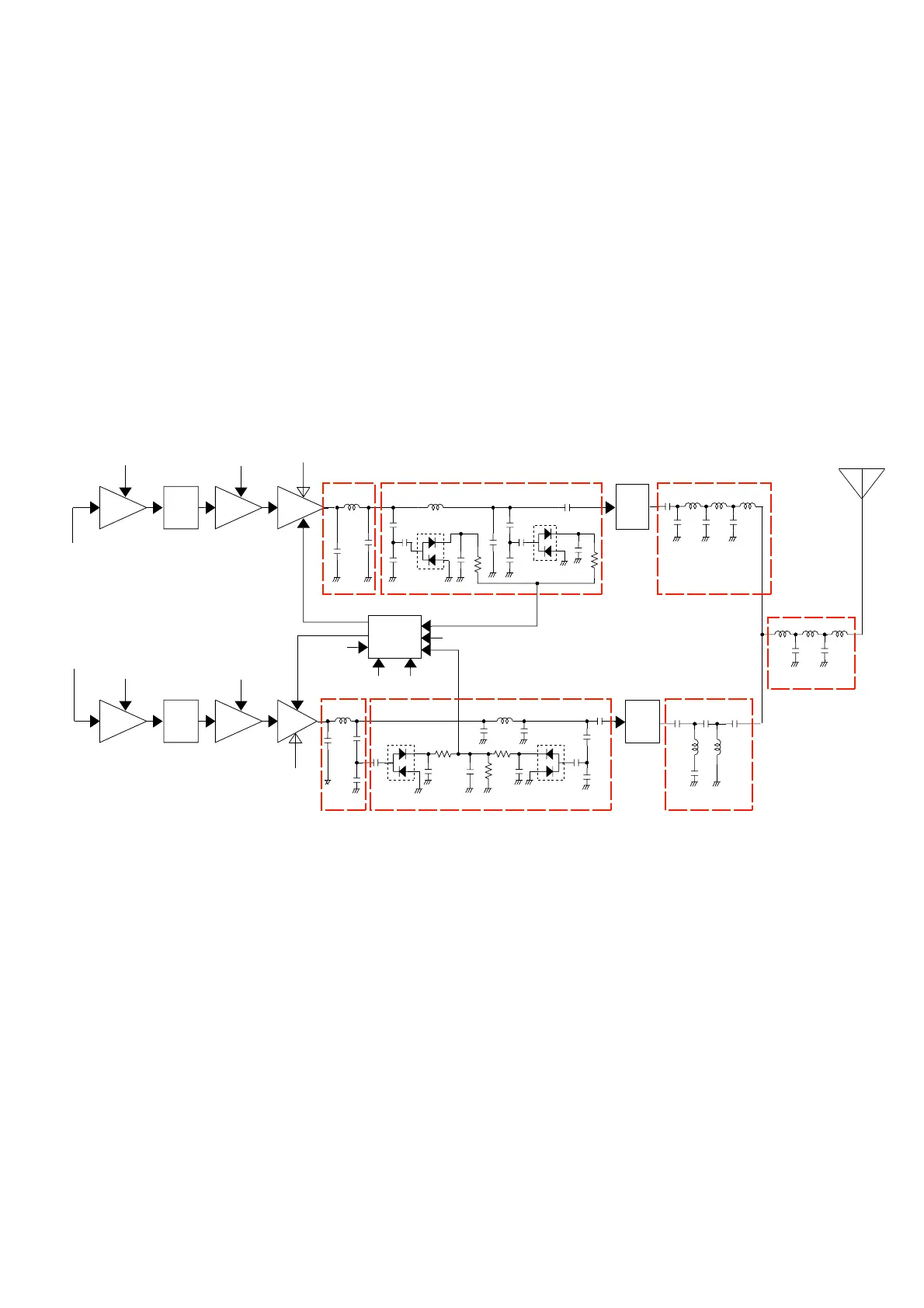
TRANSMIT POWER AMPLIFIERS
TX signal from the attenuator (R43, 47, 57) is amplifi ed by
pre-drive (Q22) and drive (Q26) amplifi ers to obtain RF level
for power module (IC2). The amplifi ed TX signal is applied
to the power amplifier which is a UHF band PA module
composed by two power MOS-FETs. The power-amplified
TX signal is passed through the LPF, power detector,
antenna switch (D62) and LPF, before being applied to the
antenna connector (CHASSIS; J1).
APC CIRCUITS
A portion of the TX signal from IC2 is rectifi ed at the power
detector (D42, 52), and converted into the DC voltage
which is in proportion to the RF power, and applied to the
operational amplifier (IC4, pin 2). IC4 is an APC amplifier
for both of V/UHF bands. The TX power setting voltage
“PCON_U” from the D/A converter (IC1, pin 6) is applied
to the pin 3 as a reference. IC4 is rolled as a differential
amplifier which outputs voltage in inverse proportion to
rectified one. When the TX power increased, the rectified
voltage also increased, that causes the decrease of output
voltage of differential amplifier. The decrease of output
voltage of differential amplifi er causes the drop of the gate
voltage of IC2, Thus the TX power maintained to keep stable
level.
TX muting is carried out by TX mute SW (Q36) controlled
by “TX_mute” signal. Applying “TX_mute” signal to the base
terminal of Q36 to turn it ON, 8 V DC appears on the pin 6 of
IC4 and its output voltage downs to 0 V DC to inactivate IC3.
L88
C326
C314
C330
L96
L92
C318
APC
CTRL
DRIVE
AMP
DRIVE
PRE PWR
AMP
D29
Q27
TX_MUTE
LIMIT
HV
RF POWER DETECTOR (VHF)
RF POWER DETECTOR (UHF)LPF HPF
LPFLPF
• APC CIRCUITS
LPF
Q25
TX signal from
LO switch (D155, D157)
IC4,Q31,Q36
IC3
PCON_U
PCON_V
TX_MUTE
VT8VT8
DRIVE
AMP
DRIVE
PRE PWR
AMP
D25
Q26
LIMIT
HV
Q22
TX signal from
LO switch (D103)
IC2
UT8UT8
L104
C342
L101
C346
L108
L77
C308
C303
C297
L80
C296
C202
C162
C227
C186
C155
C161
L46
D47
R201
L56
C198
C212
C164
C203
R154
C226
D39
C157
TX/RX
SW
D59,D75,D77
TX/RX
SW
D53,D61,D62
C224
C214
C265
D52
C174
L50
R176
L61
C173
C273
C199
C221
C231
C176
C275
C272
R166
D42
C166
R178
 Loading...