4 - 10
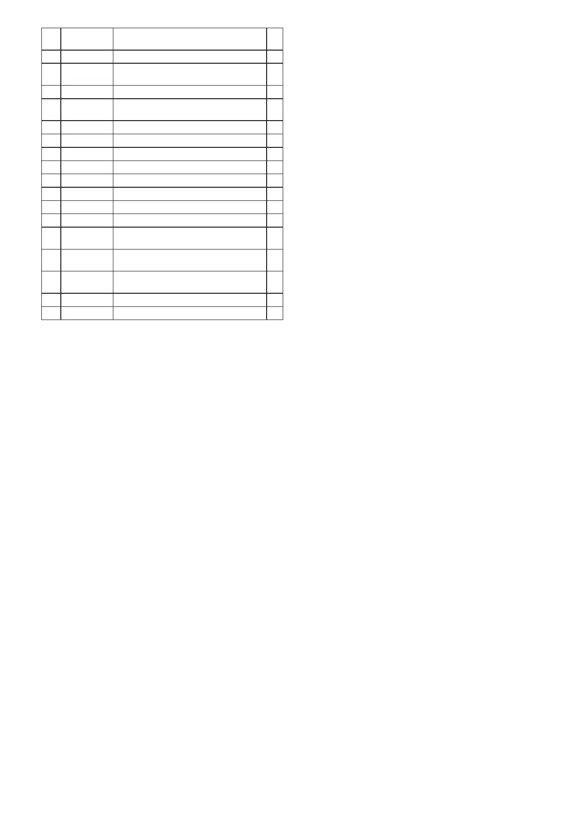
PIN
No.
PORT NAME
DESCRIPTION I/O
100
RESET
Reset enable signal input. I
101
L_SQL
Noise signal from the IF IC (Left band;
IC15).
I
102
CL_SFT2
Clock frequency shifting signal. O
105
R_SQL
Noise signal from the IF IC (Right band;
IC18).
I
122
R_DATA
Data lines for the control unit. I
123
TX_DATA
Data lines for the control unit. O
127
TX232
Data bus for RS-232C communication. O
128
RX232
Data bus for RS-232C communication. I
129
DA_CK
Serial clock signal to the D/A converter. O
130
DA_DATA
Serial data to the D/A converter. O
134
DA_STB
Strobe signal to the D/A converter. O
135
R_R5C
RX circuits (Right band) control signal. O
136
R400_S
Power line control signal to the 375−550 MHz
band RF circuit (Right band).
O
137
R_RX800
Power line control signal to the 810−1000
MHz band RF circuit (Right band).
O
138
R_AMC
AM-demodulator circuit (Right band)
control signal.
O
143
DTMSD
Data to the DTMF decoder (IC56). -
144
DTMCK
Clock signal to the DTMF decoder (IC56). -

 Loading...